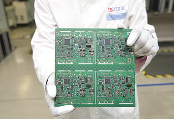
SPI : Solder paste inspection in PCB assembly
In the highly demanding and ever-evolving field of electronics manufacturing, achieving consistent quality and reliability is a fundamental objective. A critical aspect of this endeavor is the implementation of effective inspection processes, particularly during the early stages of printed circuit board (PCB) assembly. Among these, solder paste inspection has emerged as one of the most essential techniques for identifying and minimizing manufacturing defects before they propagate downstream in the production line.
Solder paste inspection plays a pivotal role in ensuring the accuracy of solder paste application, which is vital for successful component placement and long-term electronic circuit performance. Through real-time analysis and process control, manufacturers are able to evaluate paste volume, alignment, and overall printing quality directly after the stencil printing process. This early detection helps reduce the need for costly rework and ensures that each circuit board adheres to stringent quality standards.
Advancements in inspection technology, such as the integration of 3D solder paste inspection and optical inspection systems, have significantly increased the accuracy and efficiency of defect detection. These innovations enable not only the measurement of the volume of the solder paste but also the identification of anomalies such as insufficient paste, paste smearing, or offset paste. The use of solder paste inspection machines equipped with 3D measurement technology provides manufacturers with comprehensive data to optimize every manufacturing step.
As electronics manufacturing continues to scale in complexity, particularly in the context of Industry 4.0, SPI systems have become indispensable tools in achieving traceability, reliability, and compliance with international standards. This article presents a detailed examination of solder paste inspection, including its integration into the assembly process, its synergy with other inspection systems, and its overall impact on improving PCB quality and manufacturing efficiency. By understanding and optimizing each phase of the inspection process, engineers and quality specialists can significantly enhance the performance of electronic products in today’s competitive market.
In surface mount technology (SMT), solder paste printing is one of the most sensitive and influential stages of the entire assembly process. It is the initial step that directly determines the mechanical stability and electrical connectivity of the components placed on the printed circuit board (PCB). As such, it serves as a foundational manufacturing step that requires high precision and stringent control. A slight deviation in this phase such as uneven solder paste distribution, excessive deposits, or improper alignment can lead to multiple manufacturing defects that compromise the integrity of the final product.
Solder paste, a mixture of flux and fine metal particles, must be applied with uniform thickness and volume to predefined locations on the PCB through a stencil. The consistency of this application defines the eventual formation of solder joints after reflow. If the solder paste volume is too low, it may result in weak or missing connections. Conversely, excessive paste can cause bridging or short circuits. These outcomes are particularly problematic in high-density PCB assembly, where component spacing is minimal and margin for error is virtually nonexistent.
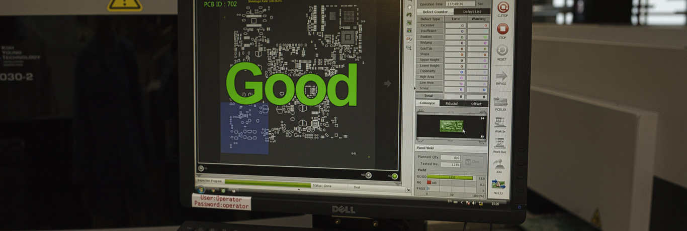
Given these challenges, solder paste inspection (SPI) has emerged as a critical solution for ensuring process reliability in modern electronics manufacturing. By providing a systematic method to inspect and measure the quality of solder paste deposits immediately after the printing process, SPI introduces a level of process control that enables early detection of anomalies. The presence or absence of solder, as well as its volume, height, and area, are among the core parameters measured by advanced SPI systems.
The introduction of SPI into the production line represents a shift from reactive to proactive quality control. Instead of waiting until final inspection stages after component placement or reflow manufacturers now have the capability to intervene much earlier. This is crucial for reducing manufacturing defects and avoiding rework, which not only affects production costs but can also delay product delivery and impact supply chain management.
Modern SPI machines rely on 3D measurement technology that offers a comprehensive view of the solder paste topography. Unlike traditional 2D systems that provide only basic silhouette or area data, 3D SPI captures volume and shape with greater fidelity, improving both the accuracy and reliability of defect detection. In this way, SPI not only enhances product quality but also facilitates data-driven decision-making in the context of Industry 4.0 and smart manufacturing environments.
Furthermore, solder paste inspection plays a vital role in traceability and quality assurance. By capturing and storing inspection data at this early stage, manufacturers can link quality metrics to specific boards, batches, and even stencil printing conditions. This level of traceability supports continuous improvement and compliance with international quality standards across the electronics industry.
Overall, the integration of SPI into the SMT assembly process strengthens the entire manufacturing workflow. It aligns with broader efforts in the electronics industry to minimize errors, optimize yield, and deliver high-quality products consistently. As this article progresses, we will delve deeper into the technical mechanisms of SPI, its relationship with surface mount processes, and its transformative impact on electronics manufacturing systems.
Solder paste inspection (SPI) is a metrological and analytical process designed to evaluate the quality of solder paste deposits applied during the early stages of printed circuit board (PCB) assembly. This process is critical in surface mount technology (SMT), where components are mounted directly onto the surface of the PCB without the use of through-hole technology (THT). Given the fine pitch of modern components and the increasing miniaturization in electronics, even the smallest deviation in solder paste application can lead to serious functional failures.
SPI functions as a real-time, inline quality assurance mechanism that evaluates the integrity of the solder paste directly after the printing process. This stage precedes component placement, making SPI the first opportunity to assess whether the solder paste application meets the geometrical and volumetric specifications necessary for forming robust and reliable solder joints. The key parameters evaluated during SPI include paste volume, height, area coverage, alignment, and the presence of any anomalies such as bridging or incomplete deposition.
By capturing this data, SPI enables manufacturers to not only detect but also understand the causes behind improper solder paste printing. It can indicate issues related to stencil quality, squeegee pressure, paste viscosity, or environmental conditions within the production line. As such, SPI does not operate in isolation; it plays a crucial role in overall process control and optimization. When integrated with statistical process control (SPC) systems, the inspection data allows engineers to make proactive adjustments, reducing the occurrence of recurring manufacturing defects.
Surface mount technology relies heavily on the accuracy and consistency of each manufacturing step. As components are placed automatically and reflowed in a thermal profile, any defect in the foundation such as an insufficient or misaligned solder paste deposit can result in missing solder joints, open circuits, or unexpected bridging. These types of defects not only reduce the performance of the electronic circuit but also increase the probability of field failure, which is especially detrimental in applications such as consumer electronics, automotive, medical devices, and aerospace.
By integrating SPI into the SMT production line, manufacturers gain early insight into the quality of each PCB and each individual solder pad. This makes it possible to catch and address defects early, long before the reflow process, where defects are harder to correct and their root causes more difficult to isolate. Furthermore, SPI contributes to greater yield, lower rework rates, and enhanced traceability features that are indispensable in today’s electronics industry, particularly under the demands of contract manufacturing and complex supply chain structures.
In essence, SPI is a cornerstone of modern SMT manufacturing. It enables high-precision control at one of the most delicate points in the assembly process, where failures can cascade downstream if not detected early. By supporting consistent solder paste application, SPI helps achieve the high quality and reliability that is expected of advanced electronic products. The next section will examine how 2D and 3D SPI techniques differ, and how the transition to three-dimensional analysis has revolutionized the inspection process in terms of both capability and confidence.
The evolution of solder paste inspection (SPI) technology has significantly influenced the ability of electronics manufacturers to evaluate and control the solder paste printing process. Initially, SPI systems employed two-dimensional (2D) inspection techniques, which provided valuable yet limited information about the solder paste deposits on the printed circuit board (PCB). Over time, with increasing demands for miniaturization and the rise of complex component geometries, three-dimensional (3D) SPI systems were introduced, offering a transformative improvement in both inspection accuracy and defect detection capabilities.
2D SPI systems primarily analyze the surface of the solder paste by capturing a top-down grayscale or color image. These systems can evaluate basic attributes such as area coverage, shape, and x-y alignment of the solder paste. However, they lack the capability to accurately measure the volume of the solder paste or the true topography of the deposits. As a result, certain defects such as excessive or insufficient paste volume, slumping, or height irregularities can go undetected using 2D inspection alone. This limitation is especially problematic in high-density SMT assemblies, where defects caused by improper solder paste printing can easily lead to bridging or missing solder joints.
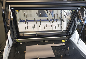
In contrast, 3D SPI systems utilize structured light projection or laser-based measurement to capture the full three-dimensional profile of each solder paste deposit. This includes precise height mapping, volume calculation, and shape reconstruction. With 3D SPI, manufacturers gain access to critical metrics such as paste volume, slope, area, and z-axis alignment, which are essential for process control and ensuring the mechanical and electrical integrity of solder joints. The ability to accurately measure the volume of the solder paste allows for more detailed process optimization and reduces reliance on assumptions or indirect estimations.
Another important distinction lies in the detection of defects. While 2D systems are effective in identifying simple defects such as misalignment or missing paste, 3D SPI machines are capable of detecting more nuanced and process-related solder paste defects, including paste smearing, insufficient paste, and volume inconsistencies due to improper stencil cleaning or environmental variations. These capabilities are especially valuable for detecting defects early and ensuring that the paste deposits are within the defined specification limits.
Moreover, 3D SPI plays a significant role in improving the overall inspection process speed and accuracy. Although 3D systems require more computational resources, modern inspection machines have been optimized to provide real-time feedback without compromising throughput. This is critical for maintaining a high-speed production line while achieving reliable inspection outcomes.
One of the key enablers of this transformation is the advancement of 3D imaging and 3D measurement technology. These innovations not only allow manufacturers to inspect more accurately, but also to implement closed-loop control systems that adjust printing parameters dynamically. As a result, the transition from 2D to 3D SPI is not merely a technological upgrade it is a fundamental shift toward a more intelligent, data-driven manufacturing environment aligned with the principles of Industry 4.0.
In summary, while 2D SPI remains a useful tool in specific contexts, the adoption of 3D SPI has become the industry standard for advanced SMT lines. The comprehensive information provided by 3D solder paste inspection enables engineers to detect defects early, improve first-pass yield, and ensure that the solder paste printing process remains stable and repeatable. This level of control is essential for meeting the strict quality and reliability requirements of the modern electronics industry.
The foundation of every surface mount technology (SMT) line is built upon the accurate application of solder paste onto the printed circuit board (PCB). This process, although often viewed as a routine step, plays a crucial role in determining the success of all subsequent assembly operations. Central to this stage are two key elements: the solder material itself and the stencil used for its deposition.
Solder is a metallic compound typically composed of tin, silver, and copper that serves as the physical and electrical connection medium between surface-mounted electronic components and the PCB pads. In its paste form, solder contains microscopic metal particles suspended in flux, which promotes adhesion and aids in the reflow process by preventing oxidation. The characteristics of the solder paste, including its viscosity, particle size, and flux activity, must be carefully controlled to ensure consistent deposition and effective wetting during reflow.
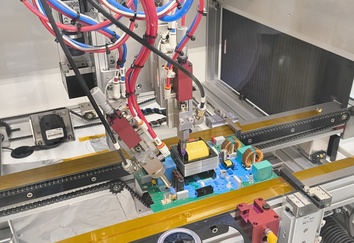
Equally important is the stencil, a precision-fabricated metal sheet that contains apertures corresponding to each solder pad on the circuit board. During the solder paste printing process, the stencil is aligned over the PCB, and solder paste is spread across its surface using a squeegee. The paste fills the apertures, and when the stencil is lifted, deposits remain on the board in the required locations. The dimensions, thickness, and quality of the stencil directly influence the volume and shape of the solder deposits, making stencil design and maintenance a key factor in achieving process consistency.
Modern inspection systems are able to measure critical characteristics of these solder deposits with high accuracy, ensuring that each pad receives the correct amount of material. This is particularly important in high-density applications, where even a small deviation in solder paste volume or placement can lead to defects such as offset paste or missing solder joints. For this reason, engineers must pay close attention to stencil cleanliness, aperture wear, and squeegee pressure, as variations in these parameters can cause defects due to improper solder paste application.
Furthermore, the stencil and solder paste process must be optimized in harmony with the component layout and pad design of the PCB. Variations in aperture shape—such as rounded versus square openings can affect paste release and transfer efficiency. In advanced manufacturing environments, the field of view (FOV) of the SPI machine must be carefully calibrated to match the board layout, ensuring the inspection system is able to measure each paste deposit accurately without distortion or overlap.
The importance of this step extends beyond initial deposition. The quality of the solder paste print directly influences the success of subsequent assembly, including component placement and the formation of reliable solder joints during reflow. Defects introduced at this stage are difficult to detect and correct after reflow, highlighting the need for robust process control and early-stage inspection. By integrating SPI systems capable of full color 3D inspection, manufacturers are able to measure accurately each deposit and identify any deviations in real-time.
In summary, the interaction between solder and stencil in the SMT assembly process is both technical and foundational. The successful execution of this stage is critical for ensuring uniform solder paste application, minimizing variability, and supporting a defect-free manufacturing process. In the context of modern electronics production, where product complexity is increasing and component dimensions are shrinking, mastering this stage is essential for maintaining high quality and yield.
In modern SMT production environments, the inspection process has become an integral manufacturing step that directly influences overall product quality, yield, and reliability. With the increasing complexity of PCB designs and the miniaturization of electronic components, inspection is no longer a passive quality control checkpoint; rather, it functions as a dynamic tool embedded within the manufacturing process to detect, evaluate, and prevent defects in real time.
The inspection process in SMT assembly typically includes several stages, beginning with solder paste inspection (SPI), followed by optical inspection after component placement, and culminating with post-reflow inspection. Each stage provides specific data points that contribute to process control and feedback loops, allowing engineers to correct deviations early. SPI, in particular, plays a foundational role, as it inspects the solder paste deposits immediately after the printing process a step where the majority of solder-related defects originate.
One of the most critical advantages of incorporating inspection early in the manufacturing process is the ability to identify and correct errors that would otherwise propagate downstream. For example, defects such as offset paste, missing solder, or irregular solder deposits can lead to improper component placement or reflow failures. These defects, if not detected promptly, may require extensive rework or cause latent failures in the field. By capturing accurate inspection data at each step, manufacturers can implement real-time corrective actions, ensuring that each PCB meets design and performance expectations.
Modern SPI machines, particularly those equipped with 3D inspection capabilities, offer an advanced level of process transparency. They are able to measure solder paste volume, height, and coverage with high precision. The introduction of full color imaging and enhanced field of view (FOV) technologies has further expanded the capabilities of inspection systems, allowing for detailed analysis of each paste deposit in a single scan. These advancements enable production engineers to evaluate the effectiveness of solder paste application with a degree of clarity previously unattainable.
Furthermore, as electronics manufacturing shifts toward automation and digitalization, the role of inspection is evolving from a quality gate to a central node in data-driven process optimization. Through the integration of SPI and AOI (automated optical inspection) systems with MES (Manufacturing Execution Systems) and SPC (Statistical Process Control) platforms, manufacturers gain access to historical trends, anomaly detection, and predictive quality insights. This holistic approach not only reduces the rate of defects but also improves traceability, a key requirement in contract manufacturing and regulated industries.
The inspection process also plays a key role in reducing rework and waste. By detecting defects early in the assembly process, manufacturers minimize the need to disassemble and repair completed boards. This has both economic and operational implications, as it conserves materials, reduces cycle times, and maintains the overall efficiency of the production line. Additionally, by ensuring uniform quality from the outset, inspection helps uphold the quality standards demanded by the global electronics industry.
In conclusion, inspection is not a separate or optional function but a fundamental part of the SMT manufacturing process. It ensures that each step from solder paste application to final assembly meets precise specifications. With advancements in SPI technology, including 3D imaging, high-speed scanning, and advanced analytics, manufacturers are now able to detect manufacturing defects early, measure accurately, and optimize their operations to deliver reliable, high-performance electronic assemblies.
Solder paste inspection (SPI) serves as one of the earliest and most decisive control points in the full assembly process of printed circuit boards (PCBs). Its role extends far beyond isolated quality control it is a strategic tool that enables proactive management of downstream outcomes in surface mount technology (SMT) environments. By evaluating the solder paste printing step in real time, SPI helps establish a reliable foundation for each subsequent operation, from component placement to reflow and final functional testing.
In a standard SMT line, the process begins with solder paste application through a stencil. At this stage, the uniformity and volume of solder paste are critical for forming dependable solder joints. SPI systems are integrated immediately after this stage to assess the quality of the deposits. Through advanced measurement techniques—especially in systems equipped with 3D inspection capabilities engineers can identify paste-related anomalies such as insufficient volume, height inconsistencies, or spatial misalignment, all of which are potential precursors to later-stage defects.
By functioning at this early stage, SPI provides inspection data that are both actionable and predictive. Instead of waiting for errors to manifest during or after component placement, manufacturers can intervene at the root cause. This predictive capability is essential for maintaining high throughput on high-volume production lines, where even minor disruptions can cascade into significant delays or yield loss. Furthermore, because SPI systems are integrated inline, they are optimized for inspection speed, enabling continuous operation without compromising process efficiency.
As the assembly process advances to component placement and reflow, the impact of the initial solder paste print becomes increasingly visible. PCBs with poor solder paste deposits are more likely to suffer from placement inaccuracies, tombstoning, bridging, or open circuits during reflow. Therefore, SPI acts as both a safeguard and a qualifier: only boards that pass this initial inspection move forward in the process. This creates a natural quality gate that enhances process flow and minimizes the need for costly rework or scrap at later stages.
Moreover, modern electronics manufacturing lines rely on feedback loops between SPI and upstream systems to enhance process stability. For instance, when a deviation is detected in the solder paste pattern, the SPI machine can trigger alerts for stencil cleaning, squeegee pressure adjustment, or environmental recalibration. These closed-loop controls contribute to the optimization of the entire manufacturing process, ensuring that each PCB maintains uniformity and alignment with design specifications.
The strategic placement of SPI within the full assembly process also supports traceability and continuous improvement efforts. Inspection data from SPI systems are often stored and analyzed in manufacturing execution systems (MES), providing engineers with historical context and trend analysis that can inform broader process optimization initiatives.
In summary, solder paste inspection is not an isolated task but a vital, embedded step in the full SMT assembly process. It enables early detection of errors, supports fast and reliable inspection cycles, and directly contributes to the delivery of high-quality PCBs. As a result, SPI plays an indispensable role in modern electronics manufacturing environments where speed, precision, and quality are equally paramount.
The integration of solder paste inspection (SPI) into the electronics manufacturing workflow marks a pivotal advancement in achieving systematic quality assurance across the entire surface mount technology (SMT) line. As production environments evolve toward greater complexity and automation, SPI systems are no longer seen as peripheral quality tools; instead, they serve as core components within digitally connected, data-driven manufacturing ecosystems.
Within a well-structured manufacturing workflow, SPI is implemented directly after the solder paste printing process and before component placement. This positioning is strategic, as it allows manufacturers to inspect and qualify the quality of solder paste deposits before any components are mounted on the printed circuit board (PCB). By evaluating parameters such as paste volume, shape, height, and area alignment, the SPI machine provides immediate feedback that enables line operators or automated systems to react to deviations in real time. This closed-loop communication between inspection equipment and process control units has become fundamental to high-efficiency electronics production.
The workflow benefits of SPI extend beyond detection and correction. Integration with broader manufacturing systems such as MES (Manufacturing Execution Systems) and ERP (Enterprise Resource Planning) platforms allows for centralized data collection and traceability. Inspection data generated by SPI machines contribute to a detailed digital profile of each PCB, enabling complete traceability from the stencil printing stage through to subsequent assembly and final test. This level of integration is particularly valuable in contract manufacturing environments, where documentation, batch control, and compliance with international quality standards are mandatory.
Furthermore, the adoption of SPI aligns closely with the principles of Industry 4.0 and smart manufacturing. Through connectivity with other automated inspection systems and machines on the line, SPI contributes to the development of an intelligent production environment that continuously adapts based on live data inputs. For example, when a deviation is detected by the SPI system, the printing process can be automatically adjusted, reducing the occurrence of recurring solder paste defects and optimizing the line’s output without human intervention.
In addition, SPI plays a key role in supporting statistical process control (SPC) across the SMT line. By continuously monitoring trends and deviations in solder paste deposition, the system helps engineers identify sources of process variation and implement long-term corrective actions. This contributes not only to better yield and product quality but also to reduced downtime and scrap rates, which are critical metrics in high-volume electronics manufacturing.
Importantly, the integration of SPI into the workflow enhances visibility and decision-making at every level of the organization. Line operators benefit from real-time alerts and visual inspection interfaces; process engineers use trend data for continuous improvement; and management can track quality performance across multiple production lines and facilities. This interconnected approach ensures that solder paste inspection contributes meaningfully to the broader goals of efficiency, consistency, and competitive advantage in the electronics manufacturing industry.
In summary, integrating SPI into the electronics manufacturing workflow transforms it from a local control function into a key pillar of the entire production strategy. It facilitates intelligent process optimization, supports comprehensive traceability, and ensures that each PCB produced aligns with rigorous performance and quality expectations demanded by today's global market.
A comprehensive understanding of each manufacturing step in surface mount technology (SMT) is essential for achieving a defect-free production flow and meeting the strict performance and reliability requirements of modern electronic devices. The sequence from solder application to final inspection includes multiple interconnected phases, each contributing to the overall integrity and functionality of the finished assembly. Each step must be carefully controlled and synchronized to ensure that potential issues are detected and resolved before they escalate into critical failures.
The process begins with solder paste application, typically performed using a stainless-steel stencil through which solder paste is deposited onto the PCB pads. This stage defines the initial physical and volumetric characteristics of the future solder joints. The correct volume and shape of the solder deposits are critical, as any deviation such as excessive or insufficient solder can lead to downstream assembly failures. Improper solder paste application is a leading cause of defects in SMT manufacturing, including bridging, tombstoning, or cold joints. Early detection of such issues is therefore essential to reduce rework and ensure yield stability.
Immediately following paste application, the solder paste inspection (SPI) stage provides the first layer of process verification. Here, SPI machines equipped with high-speed 3D inspection capabilities evaluate the quality of the solder deposits. They are able to measure a variety of parameters, including height, volume, area coverage, and alignment, with a high degree of precision. This step is designed to catch defects such as insufficient solder paste, skewed prints, or anomalies due to stencil wear. The inspection speed of these systems is optimized for high-throughput environments, enabling full inspection coverage without slowing down the production line.
Once boards pass SPI, they proceed to component placement. Here, surface-mounted electronic components are placed onto the PCB pads using automated pick-and-place machines. Proper placement is highly dependent on the quality of the underlying solder paste. Misaligned or incomplete solder deposits can cause the components to tilt, rotate, or fail to seat properly—issues that are often only visible after reflow soldering. Thus, each defect detected early by SPI reduces the risk of complex and costly errors at this stage.
Following placement, the entire board undergoes reflow soldering, during which the solder paste melts, flows, and solidifies to form permanent connections between the components and PCB. The thermal profile of the reflow process must be precisely managed to ensure optimal wetting and solder joint formation. Variations in solder paste volume or composition, which may have originated from improper stencil application, can cause incomplete joints, voiding, or other solder defects.
The final stage in the manufacturing sequence is post-reflow inspection, typically conducted using automated optical inspection (AOI) systems. These systems verify the presence, alignment, and soldering quality of each component. While AOI can detect issues such as missing components, polarity errors, or lifted leads, it is unable to correct errors introduced earlier in the process underscoring the critical role of SPI in early defect prevention.
This sequential approach starting from solder paste application, followed by SPI, placement, reflow, and AOI forms a robust quality control framework that minimizes process variation and ensures the production of high-quality PCBs. By understanding the role of each step and their interdependencies, engineers can optimize both individual processes and their cumulative impact on final product performance.
Ultimately, the integration of inspection systems throughout the manufacturing process enables early detection, precise root cause analysis, and continuous feedback. These capabilities are indispensable in high-mix, high-volume electronics manufacturing environments where even the smallest inconsistency can compromise the reliability of complex assemblies.
As the complexity of electronic products continues to grow, the precision required in PCB assembly processes has reached unprecedented levels. In this context, effective defect detection becomes a central pillar in maintaining quality and preventing failures. The adoption of three-dimensional solder paste inspection (3D SPI) systems represents a significant advancement in the electronics manufacturing industry, offering detailed insights into one of the most failure-prone stages of surface mount technology (SMT) production: solder paste deposition.
3D SPI systems utilize structured light projection or laser triangulation to perform a volumetric analysis of each solder deposit. Unlike traditional 2D systems, which provide only top-down, planar measurements, 3D SPI captures full geometric profiles including volume, height, and area allowing for more comprehensive and accurate defect detection. These capabilities are especially vital for modern PCBs, which often feature tightly packed components and increasingly miniaturized geometries. In such environments, even minute deviations in solder paste can result in critical functional defects.
Among the most common solder paste defects identified by 3D SPI systems are insufficient paste, excessive deposits, bridging, and irregular volume distribution. In many cases, these defects are due to improper solder paste application whether from clogged stencil apertures, worn edges, or inconsistent squeegee pressure. 3D SPI not only identifies these issues but also quantifies the extent of each deviation, enabling engineers to implement targeted corrective actions that prevent defect propagation to subsequent stages of assembly.
The advanced imaging systems used in modern SPI machines are also able to detect more subtle forms of defect, such as solder deposits with uneven slope profiles or those affected by environmental influences like humidity or temperature drift. Additionally, defects such as offset paste where the solder is applied in the correct volume but misaligned can be clearly visualized and measured. These inspections are conducted at high inspection speeds to ensure seamless integration into continuous production lines without impacting throughput.
The ability to measure defects with high granularity translates directly into improved process control and production efficiency. Early detection of solder paste anomalies helps reduce the number of defective PCBs advancing to component placement, reflow, or final inspection. This leads to a measurable reduction in rework, material waste, and associated labor costs. Moreover, by analyzing historical defect patterns using inspection data, engineers can refine stencil designs, adjust print parameters, and evaluate long-term equipment performance, all of which contribute to process optimization.
Another key advantage of 3D SPI lies in its contribution to the early detection of manufacturing defects that would otherwise be difficult to trace in the post-reflow stage. For example, if an electronic component fails electrical testing, root cause analysis often begins by reviewing earlier process stages. The presence of detailed SPI data, including three-dimensional profiles of each solder deposit, provides a crucial reference point for such investigations. In some cases, it may reveal that a defect occurred not during placement or reflow, but due to a flaw in the original printing process a distinction that can save valuable time and resources in high-volume manufacturing settings.
In summary, 3D SPI systems represent a transformative approach to defect detection in modern electronics production. By enabling manufacturers to inspect each solder deposit with unmatched detail, these systems enhance reliability, improve first-pass yield, and support continuous process improvement. In an era where the performance of electronic assemblies must meet ever-higher expectations, the role of 3D solder paste inspection in ensuring consistent, repeatable quality has never been more critical.
Solder paste inspection (SPI) plays a critical role in the early identification of defects that, if left unaddressed, can lead to functional failures in the final product. The majority of SMT-related failures originate from issues at the solder paste printing stage, making defect detection at this point vital to ensure reliability and reduce costs associated with rework or product recalls.
Among the most frequently encountered solder paste defects are insufficient paste, excessive deposits, bridging, and missing solder joints. Insufficient paste may result from partial aperture blockages in the stencil or inadequate squeegee pressure, leading to weak or open connections. Excessive solder, on the other hand, can cause shorts or bridging between adjacent pads, especially in high-density layouts. These defects are often due to stencil wear, excessive paste application, or incorrect environmental conditions such as humidity fluctuations.
SPI systems are also capable of identifying paste smearing, which typically results from contamination on the stencil surface or poorly controlled printing parameters. Another common anomaly is offset paste, where the solder deposit is applied in the correct volume but misaligned with the target pad. This issue can affect the accuracy of component placement and lead to cold joints or unreliable connections after reflow.
Defects caused due to improper solder paste application can further include solder balls, slumping, and volume inconsistency across the board. Each of these issues contributes to variability in solder joint formation, which directly impacts the electrical performance and mechanical strength of the final assembly. By detecting such defects early through SPI, manufacturers gain the opportunity to intervene before costly downstream errors occur.
The integration of 3D imaging into solder paste inspection has revolutionized the way manufacturers detect and respond to process deviations. While traditional 2D inspection systems are limited to analyzing planar attributes such as area and x-y alignment, 3D SPI provides full topographical data, enabling detailed volumetric analysis of each solder paste deposit.
This enhanced capability allows inspection systems to accurately measure critical parameters such as height, volume, and slope metrics that directly influence solder joint quality. For example, a solder paste deposit that appears acceptable in 2D may in fact be too low in height or uneven in shape, which would affect wetting during the reflow process. By capturing the third dimension, 3D SPI ensures that defects are not only detected but also characterized in terms of severity and potential impact.
Additionally, 3D systems often offer full color imaging, allowing for improved contrast and visual clarity when inspecting fine features or detecting subtle defects. Combined with a high field of view (FOV), these systems can scan large areas quickly while maintaining precision, which is essential in high-volume production lines. The ability to measure accurately and in detail supports more reliable process control and leads to a reduction in false calls and unnecessary interventions.
One of the greatest benefits of 3D imaging lies in its contribution to early detection. By identifying variations in solder paste volume, height, or alignment before components are placed, engineers can take corrective actions that prevent more severe issues during or after reflow. This improves first-pass yield and reduces reliance on costly post-reflow inspection and rework processes.
Ultimately, the use of 3D imaging within SPI enables a higher level of process transparency and control. It empowers engineers to optimize their printing process, detect and classify defects with greater accuracy, and make informed decisions that enhance the quality and consistency of the final electronic product.
The solder paste inspection machine is a key asset in modern electronics manufacturing environments, acting as both a monitoring tool and a corrective feedback mechanism within the SMT line. Its primary function is to identify inconsistencies in the solder paste printing process that can lead to manufacturing defects if left unchecked. By doing so, it minimizes the risk of defective assemblies entering the component placement or reflow stages.
Advanced SPI machines equipped with 3D inspection capabilities and high-speed processing are capable of inline integration, ensuring real-time analysis of every solder deposit on each PCB. These systems are designed to operate at production-level speeds, delivering comprehensive inspections without disrupting throughput. The combination of inspection speed, measurement precision, and automated classification algorithms enables rapid decision-making and immediate corrective actions.
Beyond simple defect detection, the SPI machine contributes to process optimization and quality assurance. By analyzing data across multiple boards and production batches, it can detect trends and deviations that might indicate a shift in print quality, stencil wear, or equipment misalignment. These insights allow manufacturers to proactively schedule maintenance, adjust printing parameters, or retrain personnel to prevent recurring faults.
Another critical advantage of SPI machines is their role in traceability and compliance. Each inspection generates a digital record that can be stored and linked to a specific PCB, supporting detailed analysis and regulatory reporting. In sectors such as automotive, aerospace, and medical electronics where traceability and reliability are non-negotiable the ability to document and verify each inspection step is invaluable.
In conclusion, the solder paste inspection machine serves not only as a gatekeeper against early-stage defects but also as a catalyst for continuous process improvement. Its integration into the SMT line enhances manufacturing efficiency, supports high product quality, and ensures that each board meets the rigorous standards expected in today’s electronics industry.
As surface mount technology (SMT) has matured, inspection systems have evolved into highly integrated elements of electronics manufacturing. Among these systems, optical inspection plays a complementary and synergistic role alongside solder paste inspection (SPI). While SPI is focused on the verification of solder paste deposition prior to component placement, optical inspection most often implemented as automated optical inspection (AOI) serves to assess the placement and soldering of components post-reflow. Together, these inspection systems form a layered and robust quality control framework across the production process.
Optical inspection utilizes high-resolution cameras and image processing algorithms to analyze each populated printed circuit board (PCB) for potential defects. These may include misaligned components, missing parts, incorrect polarity, or poor solder joints. Where SPI excels in catching defects early, such as insufficient solder or paste offset, optical inspection addresses issues that arise later in the process, often caused by prior undetected anomalies or mechanical misalignments during placement.
The synergy between SPI and optical inspection lies in their positioning within the process flow and their complementary inspection criteria. SPI operates pre-placement and focuses on the geometry of solder deposits, while AOI examines the final state of the assembly after reflow. This allows manufacturers to trace the origin of defects more precisely. For example, if a short circuit is identified during AOI, SPI data can reveal whether the root cause was excessive paste volume or misaligned deposition earlier in the line.
Importantly, these systems not only function as discrete inspection tools but can also be integrated into a unified inspection ecosystem. Data from SPI and optical inspection can be correlated to identify systemic process weaknesses. For example, a pattern of tombstoning or skewed components detected during optical inspection might be linked to inconsistent paste thickness measured by SPI. By leveraging both systems in concert, manufacturers achieve a more granular and accurate understanding of defect causality.
Moreover, modern inspection platforms support high-speed scanning and are designed for inline deployment, enabling real-time decision-making without slowing down the production line. As demands for inspection speed and accuracy grow in tandem, this dual-inspection approach ensures that no critical failure escapes detection, and every board is evaluated at multiple stages with different technologies.
From the perspective of process control, the combination of SPI and optical inspection enables advanced manufacturing strategies such as closed-loop correction, predictive maintenance, and continuous quality tracking. These benefits are especially relevant in high-mix, high-reliability manufacturing environments, such as those producing for the automotive, medical, or aerospace sectors.
In summary, optical inspection and solder paste inspection are not competing technologies but rather complementary pillars of modern electronics quality assurance. Their integration forms a comprehensive inspection architecture that enhances both fault detection and root cause analysis. By deploying both systems strategically, manufacturers improve their ability to maintain consistent quality, meet stringent industry standards, and respond quickly to process variability.
While both solder paste inspection (SPI) and optical inspection play vital roles in modern electronics manufacturing, they serve distinctly different purposes within the inspection process. Comparing these two systems highlights the necessity of implementing each at the appropriate stage and clarifies their contributions to overall process control and defect prevention.
SPI is employed at the very beginning of the assembly process, immediately after solder paste is deposited onto the printed circuit board (PCB). Its primary function is to assess the solder paste deposits specifically their volume, area, height, and alignment prior to component placement. By catching defects early, SPI serves as a predictive quality gate, preventing defective boards from advancing down the line.
In contrast, optical inspection, typically performed as automated optical inspection (AOI), occurs later in the process usually post-placement and post-reflow. AOI focuses on the presence, orientation, polarity, and soldering quality of electronic components. It is designed to detect visible defects such as lifted leads, missing parts, tombstoning, and misalignment. AOI systems use high-resolution cameras to capture images of the assembled board and apply image processing algorithms to compare the results against predefined standards.
The technical foundations of the two systems also differ. SPI relies heavily on 3D imaging and measurement technologies to build topographical profiles of the solder paste, while AOI depends on 2D and sometimes 2.5D vision systems to evaluate component placement and solder joint appearance. SPI is therefore more effective in detecting early-stage print-related anomalies, whereas AOI is essential for verifying final assembly correctness.
In evaluating these systems, it's important not to view them in isolation or competition. Instead, their value lies in how they complement each other. A defect missed during SPI such as a misaligned deposit might manifest as a solder bridge detected during AOI. Likewise, a defect identified during AOI may prompt a root cause investigation into the solder printing process, traceable through SPI data. Each system strengthens the other by filling gaps in inspection coverage, resulting in a more complete and reliable quality assurance framework.
The integration of 3D SPI and optical inspection represents a powerful approach to achieving high-precision, end-to-end inspection in SMT manufacturing. When these systems are combined within a cohesive inspection strategy, manufacturers benefit from layered data collection, improved fault localization, and more comprehensive quality coverage.
3D SPI provides quantitative, metrological data on the physical properties of the solder paste before any components are introduced to the PCB. This includes measurements of paste volume, height, area, and the uniformity of each deposit. These measurements enable engineers to assess not only the presence of solder but also its readiness to form reliable solder joints. Using volumetric data, process engineers can detect and correct subtle shifts in print consistency that would not be visible through traditional 2D inspection methods.
Once components are placed and soldered, optical inspection takes over by analyzing the final state of the assembly. With the use of advanced lighting techniques and image recognition algorithms, AOI systems evaluate the quality of component mounting, the presence of unwanted bridging or tombstoning, and the formation of acceptable solder joints. While AOI cannot measure solder volume, it can effectively flag visible signs of improper soldering or misplaced components.
When these two inspection methods are deployed in concert, manufacturers gain the ability to trace defects across multiple stages of production. For example, a component defect found during AOI can be linked back to variations in solder height or misalignment detected during SPI. This feedback loop not only enhances fault diagnosis but also supports closed-loop correction mechanisms, wherein printers or pick-and-place machines can adjust their parameters automatically in response to inspection feedback.
Moreover, combined inspection data from SPI and AOI can feed into higher-level systems, such as MES or SPC platforms, for statistical process analysis and yield optimization. This capability is particularly important in large-scale, multi-line operations, where granular process insights and high-quality consistency are critical performance indicators.
In conclusion, the strategic combination of optical inspection and 3D SPI leads to significantly improved inspection coverage and accuracy. By integrating these technologies effectively, electronics manufacturers can ensure that each stage of production is monitored, controlled, and continuously optimized to meet the rigorous quality standards of today’s electronics industry.
The combined use of solder paste inspection (SPI) and optical inspection technologies provides numerous strategic and operational advantages for electronics manufacturing services (EMS) providers. These benefits are not limited to improved product quality; they extend to process stability, cost efficiency, customer satisfaction, and long-term competitiveness in a global marketplace.
For EMS providers, operating under strict timeframes and diverse product requirements, inspection systems offer a means of standardizing quality across multiple production lines and product types. By integrating SPI and optical inspection at key stages of the surface mount technology (SMT) process, manufacturers can establish repeatable control mechanisms that detect and prevent defects before they escalate into costly failures. This is especially important in environments where high-mix, low-volume production is common, and each batch may present different technical specifications and risk profiles.
One of the most tangible benefits of this dual-inspection strategy is the reduction of rework. Early detection of solder-related issues, such as insufficient paste, misalignment, or bridging, minimizes the number of defective units that proceed to later stages of assembly. This not only conserves materials and labor but also shortens production cycles and improves delivery timelines factors that are critical in contract manufacturing and supply chain management scenarios.
Moreover, by deploying both SPI and AOI systems, EMS providers enhance their ability to meet quality standards imposed by end customers or regulatory bodies. These systems offer traceable inspection records that can be used to verify compliance, support audits, and resolve quality disputes. In sectors like consumer electronics, automotive, and aerospace, where product reliability and documentation are paramount, the ability to demonstrate process traceability is a significant differentiator.
The adoption of advanced inspection systems also supports broader process optimization initiatives. Data collected from SPI and AOI can be aggregated, analyzed, and fed into statistical process control (SPC) systems, enabling proactive adjustments to stencil printing, component placement, or thermal profiles. This results in more consistent yields and fewer manufacturing defects, ultimately improving the financial and operational efficiency of EMS providers.
Finally, the combination of SPI and optical inspection aligns with the goals of Industry 4.0, where interconnected systems share data across the production ecosystem. For EMS companies aiming to build smart manufacturing systems, this dual-layered inspection architecture serves as a critical enabler. It facilitates real-time decision-making, predictive maintenance, and continuous process improvement all essential for remaining competitive in a rapidly evolving electronics industry.
In essence, the integration of SPI and optical inspection delivers measurable value to EMS organizations, not only by enhancing product quality but by transforming inspection into a strategic asset that drives process excellence and customer trust.
The electronics manufacturing industry has undergone a rapid transformation driven by the integration of advanced inspection technologies. These innovations have redefined the standards of quality control and contributed significantly to the evolution of manufacturing services. As market demands for miniaturization, speed, and complexity continue to rise, the role of inspection machine technologies becomes increasingly central to maintaining competitiveness, efficiency, and consistency across production lines.
One of the most impactful developments has been the implementation of high-resolution, high-speed solder paste inspection machines capable of 3D measurement. These machines enable manufacturers to detect solder paste anomalies with high precision and minimal latency, allowing for real-time adjustments. Through structured light projection and laser triangulation, such systems can generate full 3D profiles of solder deposits, offering insights into their geometry, volume, and placement accuracy. This capability is particularly critical for detecting early-stage printing defects that may otherwise go unnoticed but can result in costly failures if allowed to progress downstream.
Beyond the SPI domain, automated optical inspection (AOI) systems have also seen significant advancements. These machines now feature enhanced imaging, AI-based defect classification, and machine learning algorithms that reduce false calls and improve fault detection rates. In combination with SPI, they provide a multi-layered defense against a broad spectrum of assembly-related defects. This holistic approach enhances the ability of electronics manufacturing services (EMS) providers to deliver products that meet stringent industry standards and customer specifications.
The role of automation and AI in inspection systems has grown in parallel with these hardware advancements. Modern inspection machines can now perform self-calibration, adapt inspection criteria based on product type, and initiate corrective actions through machine-to-machine communication. These capabilities are essential for manufacturers operating under the principles of smart manufacturing or Industry 4.0, where every element of the production line is expected to generate and respond to actionable data.
For manufacturing services, the adoption of such inspection machines yields numerous advantages. These include reduced rework, faster time-to-market, improved customer satisfaction, and the ability to support complex products with tight process windows. Additionally, the traceability offered by digital inspection systems supports compliance, internal audits, and long-term data retention, which are increasingly critical in regulated industries.
Looking ahead, the future of inspection machines points toward even greater integration and intelligence. The use of 3D SPI machines with enhanced resolution, broader field of view (FOV), and full color image processing will further improve the detection of edge-case defects. Moreover, emerging capabilities in deep learning will enable systems to differentiate between true defects and acceptable variations based on historical production patterns, enabling a more nuanced understanding of quality and risk.
In summary, advanced inspection machine technologies are reshaping the landscape of manufacturing services in the electronics industry. By enabling early, accurate, and automated defect detection, they empower EMS providers to meet growing complexity and quality demands while optimizing their operational efficiency. As the industry continues to evolve, the role of inspection will shift from quality control to strategic enabler driving innovation, differentiation, and sustained excellence in electronics manufacturing.
Choosing the appropriate solder paste inspection machine for a specific assembly line is a strategic decision that impacts not only inspection accuracy but also process flow, throughput, and long-term operational efficiency. With the increasing variety of SPI technologies available on the market, selecting a system that aligns with the technical and production requirements of a given SMT environment requires careful consideration of several interrelated factors.
First and foremost, the resolution and measurement capabilities of the SPI machine must match the complexity of the board design and the size of the solder deposits. For high-density PCBs with fine-pitch components, machines that offer 3D inspection capabilities and precise volumetric analysis are essential. These systems provide accurate data on solder height, volume, and shape, allowing for early detection of issues that could compromise reflow performance and overall assembly integrity.
Another key factor is inspection speed. In high-volume manufacturing environments, SPI systems must be capable of inspecting thousands of solder pads per minute without creating bottlenecks in the production line. Systems with high-speed scanning, wide field of view (FOV), and optimized processing algorithms ensure that quality control does not come at the expense of throughput.
Additionally, integration capabilities play a crucial role. Modern SPI machines should be compatible with upstream and downstream equipment, as well as with factory-wide data systems such as MES and SPC platforms. This connectivity enables real-time feedback and closed-loop control, which are essential for achieving consistent, automated quality management.
Usability and adaptability are also important. The selected machine should offer user-friendly software interfaces, customizable inspection criteria, and the flexibility to accommodate various board sizes and product configurations. These features support rapid changeovers and simplify operation in high-mix manufacturing environments.
Ultimately, selecting the right SPI machine requires a balance between technical precision, operational efficiency, and long-term scalability. By aligning machine capabilities with specific production needs, manufacturers can enhance defect detection, improve yield, and maintain high standards of process control across the assembly line.
The integration of automation and artificial intelligence (AI) into modern inspection systems has redefined how quality assurance is approached in electronics manufacturing. These technologies enable inspection platforms not only to detect defects but also to understand process patterns, adapt in real time, and support intelligent decision-making across the production line.
Automated inspection systems, such as SPI and AOI machines, are now equipped with features that enable full self-calibration, automatic threshold setting, and seamless machine-to-machine communication. These capabilities reduce dependency on manual adjustments and allow for high levels of repeatability and consistency, even in fast-paced, high-mix environments.
AI adds an entirely new dimension to this automation. Through machine learning algorithms trained on vast datasets of solder paste and component images, inspection systems can distinguish between true defects and acceptable variations. This reduces false positives and enables more nuanced classification of process anomalies. AI-driven systems are able to measure the context and behavior of deviations rather than applying rigid pass/fail rules, thus improving both accuracy and efficiency.
Another key benefit of AI in inspection is predictive analytics. By analyzing historical inspection data, AI can identify emerging patterns that may indicate stencil wear, nozzle misalignment, or shifts in paste viscosity. These insights allow for proactive maintenance, early process intervention, and long-term process optimization all without human prompting.
Furthermore, AI enhances traceability and compliance by supporting intelligent data organization and reporting. Inspection results are automatically linked to specific boards, batches, and timestamps, facilitating root cause analysis and regulatory auditing. In industries where traceability is essential, such as automotive, aerospace, and medical electronics, this functionality provides significant added value.
As electronics manufacturing continues to evolve, the convergence of automation and AI in inspection systems will play a central role in building reliable inspection frameworks that are faster, smarter, and more adaptive than ever before.
As the electronics industry continues to push the boundaries of complexity and miniaturization, the future of inspection of PCB and solder paste is being shaped by several key technological and methodological trends. These developments aim to enhance inspection precision, increase speed, and enable deeper integration with digital manufacturing ecosystems.
One prominent trend is the evolution of 3D measurement technology. Future SPI systems will offer even higher resolution, faster processing, and improved adaptability to different PCB geometries. These machines will support dynamic FOV adjustment and real-time correction capabilities, further enhancing the accuracy of solder paste evaluation. Combined with full color imaging and advanced 3D reconstruction algorithms, these technologies will deliver richer, more actionable inspection data.
Another significant trend is the deeper integration of inspection systems into smart factory environments. As part of manufacturing systems driven by Industry 4.0 principles, future SPI and AOI machines will act as nodes within interconnected networks, exchanging data not only with MES platforms but also with design tools, printers, and placement machines. This will allow for immediate response to deviations, as well as continuous alignment between design intent and production reality.
AI and deep learning will continue to expand their role, particularly in automated classification and real-time process adaptation. Inspection systems will become increasingly autonomous, capable of learning from new product types, recognizing subtle defect signatures, and adjusting inspection parameters on the fly.
Finally, the emphasis on sustainability and cost-efficiency will push manufacturers to implement systems that reduce false calls, minimize material waste, and lower power consumption. These inspection innovations will support greener and more resilient production processes while maintaining the high standards of PCB quality required in today's competitive global market.
In conclusion, the future of solder paste and PCB inspection lies in enhanced resolution, smarter systems, and tighter integration. These advancements will equip manufacturers with the tools necessary to meet growing demands for quality, traceability, and operational excellence in the next generation of electronic assemblies.
The implementation of solder paste inspection (SPI) in surface mount technology (SMT) manufacturing represents a strategic advancement in quality assurance and process optimization. As the complexity of electronic assemblies increases and the tolerances for error become narrower, SPI has evolved from a supporting process to a core pillar of manufacturing control. Its ability to evaluate solder paste deposits in real time provides engineers and operators with the visibility and precision necessary to maintain consistent output quality across all production volumes.
Throughout this article, we have examined the role of SPI within the broader context of SMT manufacturing from the fundamentals of stencil printing and solder paste behavior to the technical capabilities of modern 3D SPI machines. It is clear that early detection of anomalies in solder paste application has a direct and significant impact on the quality of subsequent assembly steps, including component placement, reflow, and final inspection. By integrating SPI systems at the correct point in the assembly line, manufacturers are able to reduce defect rates, minimize rework, and improve overall process stability.
One of the most effective ways to implement SPI is by ensuring alignment with the specific requirements of the manufacturing process. This includes selecting machines with appropriate measurement resolution and inspection speed, integrating them with MES and SPC platforms, and configuring them to support inline process control. Furthermore, the combination of SPI with optical inspection and other quality systems enhances defect detection coverage and enables closed-loop feedback mechanisms that are vital for continuous improvement.
Best practices also include establishing data-driven decision-making protocols. The information collected by SPI systems should not be used in isolation but rather combined with downstream inspection data and manufacturing performance metrics. This approach supports traceability, root cause analysis, and long-term process development. Additionally, fostering cross-functional collaboration between quality engineers, process specialists, and production teams ensures that SPI findings translate into meaningful actions on the shop floor.
From a technological standpoint, leveraging advanced features such as 3D imaging, full color visualization, and automated classification helps ensure that even the most subtle defects such as insufficient paste, solder deposits misalignment, or defects such as offset paste are consistently detected and addressed. These innovations support the broader goals of manufacturing step control, defect prevention, and yield enhancement.
Finally, as part of a modern, connected manufacturing environment, SPI contributes to broader initiatives in traceability, process control, and quality and reliability. Its role is not confined to inspection alone but extends to enabling smarter, faster, and more agile production systems capable of delivering high-performance electronic products in line with the rigorous standards of today’s global electronics industry.
In conclusion, implementing SPI effectively within SMT manufacturing is not simply a technical decision, but a strategic commitment to excellence. By adopting best practices, aligning technologies with production needs, and continuously evolving inspection strategies, manufacturers can ensure long-term quality, operational efficiency, and customer satisfaction across the electronics supply chain.