ICT - in-circuit test
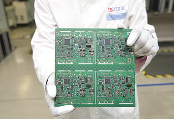
In the rapidly evolving landscape of electronics manufacturing, where product complexity and miniaturization have reached unprecedented levels, ensuring the quality and reliability of electronic assemblies has become a critical requirement. Among the various testing techniques employed to meet these demands, the In-Circuit Test (ICT) stands out as a foundational method used to verify the functionality and integrity of assembled printed circuit boards (PCBs). The ICT process plays a vital role in detecting manufacturing defects at an early stage, thereby safeguarding downstream processes and enhancing the overall reliability of electronic products.
The in-circuit test is a widely adopted testing method in the electronics manufacturing sector, particularly within the domains of Surface Mount Technology (SMT), Through-Hole Technology (THT), and PCB assembly. By providing direct electrical contact with test points on the PCB, ICT allows engineers to thoroughly examine the integrity of solder joints, component placement, and electrical connections. Unlike other forms of testing such as functional test, which assess the board’s behavior under simulated operating conditions, ICT focuses specifically on the verification of individual components and circuit continuity at the assembly stage. This distinction underscores the essential role of ICT in delivering reliable testing outcomes before a board progresses to system-level validation.
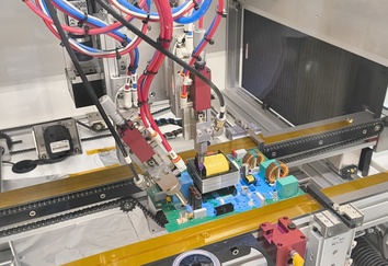
Modern ICT systems utilize sophisticated test equipment and probes to interface with meticulously designed test points on the PCB. These probes or test pins establish electrical pathways to critical nodes, enabling automated measurement of resistance, capacitance, inductance, and other electrical properties. High-density boards with complex PCB designs often require the use of in-circuit test fixtures—custom mechanical structures designed to maintain precise contact with test points while ensuring efficient and reproducible testing cycles. For boards where physical access is limited, alternative solutions such as flying probe testing provide a dynamic and flexible method to achieve comprehensive PCB testing without the need for a dedicated fixture and test infrastructure.
The emergence of different types of ICT, including both bed-of-nails and flying probe systems, has enabled manufacturers to tailor their test strategies to the specific needs of each product line. Whether dealing with high-volume production or low-volume, high-mix environments, ICT provides a scalable and adaptable solution for accurate testing and defect detection. Furthermore, the integration of ICT with other specialized testing techniques such as boundary scan testing enhances its capability to detect faults that may otherwise remain hidden.
Understanding the principles, methodologies, and implementation strategies behind ICT is essential for anyone involved in electronics manufacturing, PCB assembly, and quality assurance. This article presents a comprehensive exploration of in-circuit test systems, including their components, testing processes, advantages, limitations, and future trends. By delving deeply into the use of ICT and its application across various manufacturing contexts, we aim to provide a definitive resource for engineers, quality managers, and technical professionals seeking to optimize their testing methodologies and ensure the reliability of the PCB at every stage of production.
The In-Circuit Test (ICT) is a testing method employed during the manufacturing of electronic assemblies to evaluate the integrity of individual components and the overall electrical network on a printed circuit board (PCB). Rather than assessing the operational behavior of the assembled device, ICT focuses on identifying manufacturing defects such as open circuits, short circuits, soldering faults, and incorrect component values. This targeted approach enables the early detection of errors that, if left unaddressed, could compromise the reliability and functionality of the final product.
During an in-circuit test, a dedicated test fixture equipped with test probes or needles establishes electrical contact with test points strategically placed across the PCB. These test points are either pads, vias, or component leads designed explicitly to facilitate testing. The ICT process typically involves automated measurements of resistance, capacitance, inductance, and diode behavior, verifying the presence, orientation, and correct value of components. By accessing multiple test points on the board, the ICT system ensures that every critical element within the circuit is individually evaluated, significantly enhancing test coverage.
One of the distinguishing characteristics of ICT is its capacity for high-volume testing, making it particularly valuable in mass production settings. By enabling efficient testing and rapid identification of faults, ICT reduces the risk of defective products reaching the market. Furthermore, ICT provides quantitative data that can be leveraged for process optimization and continuous improvement initiatives in electronics manufacturing.
Although both ICT and functional test are integral components of comprehensive quality assurance strategies, they serve fundamentally different purposes within the testing process. Understanding the distinction between these two methods is essential for implementing effective test strategies tailored to specific manufacturing and product requirements.
The in-circuit test is designed to verify the correctness of individual components and interconnections on the PCB immediately after the assembly process. It ensures that resistors, capacitors, integrated circuits, and other discrete elements are properly installed, free of defects, and electrically sound. ICT checks each component in isolation without necessarily powering the entire board, minimizing the risk of cascading failures during the testing process.
In contrast, the functional test evaluates the fully assembled board by simulating its intended operating environment. It examines the collective behavior of the circuit under real-world conditions, ensuring that all systems interact correctly to deliver the desired functionality. While the functional test provides an end-to-end validation of the board’s performance, it may not detect underlying issues at the component level that ICT can uncover.
The choice between ICT vs functional test is not binary; rather, they are complementary techniques. Employing various test approaches sequentially starting with ICT to catch early assembly defects, followed by functional testing for holistic verification results in a more reliable testing strategy. This layered approach enhances the quality and reliability of the final product, minimizing warranty costs and increasing customer satisfaction.
In the context of PCB assembly, the use of ICT is pivotal for maintaining high standards of product quality and process efficiency. Given the increasing complexity of PCB designs, characterized by fine-pitch components, high component densities, and multi-layer structures, achieving thorough PCB testing has become more challenging than ever before. ICT offers a robust solution to these challenges by enabling the systematic examination of each element on the board.
During PCB assembly, once components are placed and soldered onto the board, the PCB is subjected to in-circuit testing using either a bed-of-nails test fixture or, in cases where board accessibility is limited, flying probe testing. Bed-of-nails fixtures provide rapid and simultaneous access to hundreds or thousands of test points on the PCB, making them ideal for high-volume testing environments. Conversely, flying probe systems offer flexibility for low- to medium-volume production, eliminating the need for custom fixtures.
ICT requires careful planning during the pcb design phase, often referred to as design for test (DFT). By incorporating accessible test points, ensuring sufficient spacing between components, and considering fixture constraints, engineers can significantly improve test coverage and reduce testing costs. Effective test program development is equally critical, involving the creation of software routines that automate measurements, diagnose faults, and generate actionable data.
The integration of ICT into the overall manufacturing workflow not only helps in detecting defects but also supports system-level testing and validation efforts. By identifying and rectifying issues early in the testing process, manufacturers can ensure that the reliability of the PCB is maintained throughout the product lifecycle. In doing so, they strengthen their competitive position in the marketplace by delivering products that meet the highest standards of quality and performance.
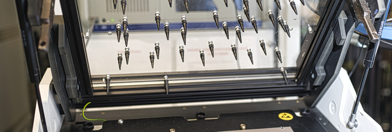
Traditional In-Circuit Test (ICT) systems have long been a cornerstone of electrical testing in electronics manufacturing. Typically utilizing a bed-of-nails test fixture, these systems are designed to make electrical contact with test points spread across the surface of the printed circuit board (PCB). The fixture, integrated with a test system, places hundreds or thousands of spring-loaded pins at precise locations, establishing robust electrical pathways for component-level analysis.
This form of specialized testing offers efficient testing for high-volume production environments, where speed, repeatability, and thoroughness are paramount. By connecting the PCB to specialized testing equipment, traditional ICT setups automate the validation of critical parameters such as resistance, capacitance, transistor orientation, and circuit continuity. The combination of mechanical precision and software-driven automation ensures that every test point is accurately probed, delivering exhaustive data on the integrity of the assembly.
Moreover, traditional ICT systems are capable of multiple test operations simultaneously, such as checking component values while verifying solder joint quality. This parallelism enhances throughput and significantly reduces cycle times, making traditional ICT highly suitable for industries where high-volume testing is essential to meet market demands. However, the initial investment in test fixtures and the associated costs of fixture maintenance must be considered during system selection.
While traditional ICT remains indispensable for mass production, the advent of flying probe testing introduced a more adaptable testing method, particularly suited for prototyping, low- to medium-volume runs, and complex PCB designs where fixture costs are prohibitive. Unlike bed-of-nails systems, flying probe testers use multiple movable probes that are robotically guided to contact test points on the board without the need for a dedicated fixture.
Flying probe testing allows for direct access to even the most densely packed areas of a PCB, providing an unparalleled level of flexibility. These systems can easily adapt to board design changes, making them ideal for industries requiring rapid design iterations or customized product variants. Although flying probe systems typically have longer test times compared to traditional ICT due to their sequential probing nature, the elimination of fixture costs and the ability to test without physical redesign make them an invaluable asset in dynamic manufacturing environments.
In addition, flying probe systems can execute advanced test functions, such as vectorless testing and boundary scan techniques, further expanding their coverage capabilities. They are particularly beneficial when physical access to test points on the PCB is limited, and when high pin-count devices are employed. Despite their slower speed relative to bed-of-nails testers, flying probe testing ensures comprehensive PCB testing without sacrificing diagnostic accuracy.
Choosing between ICT test and flying probe testing depends largely on production volume, product complexity, and lifecycle stage. In environments where a high number of identical boards must be tested quickly and reliably, traditional ICT with bed-of-nails fixtures remains the most effective solution. Its capability for high-volume testing, combined with minimal per-unit test costs after fixture amortization, makes it ideal for mass production lines.
Conversely, flying probe testing offers substantial advantages for small series production, prototypes, or products undergoing frequent design changes. It minimizes upfront investment and shortens the time to market by removing the need to design and manufacture custom in-circuit test fixtures. Furthermore, flying probe systems can easily adapt to various board revisions, providing the necessary agility for fast-paced product development cycles.
From a test coverage perspective, both systems are highly capable, but with differing strengths. Traditional ICT testers excel at rapid, parallelized testing across a wide array of test points, while flying probe systems offer finer-grained access to challenging locations and allow for real-time adjustments in probing strategies. Importantly, testing can help ensure the detection of subtle manufacturing defects that might otherwise escape notice, safeguarding product quality before system integration.
In conclusion, while test vs selection should be guided by project-specific factors such as cost constraints, design complexity, and production volume, a combined approach leveraging both ICT and flying probe techniques can often deliver the most comprehensive testing coverage and manufacturing flexibility.
The ICT process is a meticulously structured sequence of operations designed to verify the electrical and assembly integrity of a printed circuit board (PCB) immediately after the completion of PCB assembly. By systematically examining each component and electrical path, the in-circuit test offers a crucial layer of quality assurance that helps to ensure that the PCB is free from manufacturing defects and ready for subsequent integration or system-level evaluation.
The typical testing process begins with preparing the PCB by placing it into a specially designed test fixture. This fixture ensures stable mechanical positioning and precise contact with test points distributed across the board. The ICT equipment then applies test signals through test probes, checking for open circuits, shorts, incorrect components, misoriented parts, and other assembly defects. The entire procedure is automated and controlled by a test program that specifies the exact sequence and parameters of each measurement.
One of the strengths of the ICT process is its ability to identify faults early in the production cycle. By isolating defective assemblies before further investment in additional processing or system testing, manufacturers can dramatically reduce costs, improve yields, and enhance the overall reliability of their products. Importantly, ICT involves both analog and digital testing techniques to achieve broad diagnostic coverage.
A fundamental element of the in-circuit test system is the test fixture, often referred to as the "bed-of-nails." The fixture and test infrastructure is responsible for maintaining precise alignment between the PCB and the test probes, enabling consistent and repeatable electrical connections to the test pads or test points designed into the board.
Designing an effective ICT fixture is a specialized engineering task that demands a thorough understanding of the PCB design, including component placement, signal routing, and mechanical constraints. The goal is to create a fixture that not only provides reliable electrical contact with test points but also minimizes mechanical stress on the board during the testing cycle.
Modern test equipment that places test probes with high precision uses advanced fixturing technologies such as pneumatic or vacuum-assisted clamps to secure the board. The test fixture must accommodate considerations such as the location of tall components, fragile parts, and flex-sensitive areas. Access to multiple test points across different board layers requires intricate probe arrangements and sometimes double-sided probing.
The success of the ICT is heavily dependent on the quality of the test fixture. A poorly designed fixture can result in inconsistent contact, false failures, or even damage to the PCB. Therefore, fixture design is often tightly integrated with test program development to ensure seamless operation and maximum test coverage.
Test program development for ICT is a critical phase that transforms the physical design of the PCB and the test fixture into an executable set of instructions for the test system. An effective test program coordinates the operation of probes, defines the electrical measurements to be taken, and establishes pass/fail criteria based on the expected behavior of components and circuits.
This process starts with a comprehensive analysis of the PCB design files, including schematics, netlists, and bill of materials (BOM). Engineers identify all accessible test points and map them to specific measurements. Strategies such as design for test ensure that the board layout optimizes accessibility for probing and simplifies the programming effort.
Key aspects of test program development include:
Verification of correct component values and placements
Detection of opens and shorts in the circuit
Validation of power and ground continuity
Analysis of passive and active components under static conditions
Advanced ICT testers may also support techniques like vectorless testing, where the presence and correct orientation of components such as ICs are verified without direct functional stimulation. In addition, boundary scan integration allows for testing of high-pin-count devices without needing physical probe access to every pin.
An effective test program not only identifies failures but also provides detailed diagnostic information to aid in rapid troubleshooting and repair. By developing robust test routines tailored to the product’s complexity and criticality, manufacturers ensure that ICT can detect defects with a high degree of accuracy, contributing to overall reliable testing and process optimization.
Modern ICT test systems represent an advanced fusion of hardware and software, designed to conduct comprehensive electrical evaluations of printed circuit boards (PCBs) during electronics manufacturing. At their core, these systems automate the measurement and analysis of circuits, ensuring that each component performs within specified parameters before system-level integration.
A typical ICT system consists of several critical components: a test fixture, an array of precision test probes, measurement instrumentation, switching matrices, and a powerful software environment for test program development. The test system interfaces with the PCB by making electrical contact with test points, enabling high-throughput and high-accuracy verification of circuit continuity, component values, polarity, and correct installation.
One of the distinguishing features of ICT equipment is its capability to conduct multiple test operations simultaneously across a large number of nodes. This parallel testing approach significantly reduces total test time, making it ideally suited for high-volume testing applications. Additionally, the integration of analog and digital testing modules within a single platform allows for both passive and active component analysis without changing test configurations.
Modern ICT testers also support emerging testing requirements, such as boundary scan protocols and vectorless measurements, allowing them to adapt to the demands of increasingly complex PCB designs. By using test equipment that places test probes with micron-level accuracy, contemporary ICT solutions ensure that even densely packed or miniaturized boards can be tested reliably and efficiently.
Selecting appropriate test equipment for an ICT application requires a detailed understanding of the product’s characteristics, production volume, and testing requirements. Several key factors influence the decision-making process:
First and foremost, test coverage capabilities must align with the design complexity of the PCB. Boards with a high component count or fine-pitch devices demand test systems capable of high-density probing and advanced diagnostic features. The ability to make precise and consistent contact with test points is crucial to minimize the risk of intermittent faults or missed detections.
Second, the adaptability of the test equipment is critical. In fast-moving industries where products undergo frequent revisions, the flexibility to modify or update test programs quickly can dramatically impact time-to-market. Features such as programmable switching matrices and modular instrumentation expand the testing envelope without requiring extensive hardware reconfigurations.
Third, the scalability of the ICT system must match the projected production volumes. While flying probe solutions might suffice for low- to mid-volume production, dedicated bed-of-nails testers equipped with high-speed analyzers are better suited for high-volume testing environments where throughput is paramount.
Finally, reliability and maintainability of the test equipment play essential roles in sustaining operational efficiency over time. Robust mechanical design, comprehensive self-diagnostic capabilities, and vendor support structures contribute to minimizing downtime and ensuring consistent testing performance across production shifts.
Maintaining the accuracy and reliability of ICT equipment requires systematic calibration and preventive maintenance protocols. Over time, the mechanical elements of the test fixture and the sensitivity of measurement instruments can degrade, potentially compromising the precision of the testing process.
Regular calibration procedures involve verifying the performance of test probes, analog and digital measurement circuits, switching elements, and the fixture alignment mechanisms. By ensuring that the equipment that places test probes remains within specified tolerances, manufacturers can maintain the accurate testing needed to detect subtle defects that could otherwise escape notice.
Preventive maintenance activities include inspecting for worn or damaged probes, cleaning the fixture interface to prevent contamination, and updating firmware or software to incorporate the latest enhancements and bug fixes. Given the critical nature of electrical contact with test points, even minor degradation in probe performance can lead to false negatives or unnecessary rework costs.
Proper calibration and maintenance not only sustain reliable testing results but also extend the operational lifespan of expensive ICT testers and test equipment. By adopting a structured maintenance strategy, electronics manufacturers ensure that their testing methodologies remain robust, efficient, and capable of supporting evolving product requirements.
In the realm of electronics manufacturing, achieving comprehensive test coverage is fundamental to ensuring the overall quality and reliability of electronic products. ICT covers a broad spectrum of possible manufacturing faults by automating the testing of individual components, solder joints, and electrical connections. Effective measurement of test coverage involves assessing how many nets and components on a printed circuit board (PCB) are actually being verified during the ICT process.
The term "test coverage" generally refers to the percentage of the PCB’s nets, components, and functional blocks that are directly assessed during the testing process. High test coverage rates imply a lower likelihood of undetected faults proceeding to later production stages. Critical aspects include the ability to verify the correct installation and electrical behavior of components on a printed circuit, and the accessibility of test points necessary for probing.
A well-designed ICT system optimizes test coverage by strategically locating test points and tailoring the test program to the board’s architecture. Testing is typically conducted in both unpowered and powered states to maximize fault detection capabilities without introducing the risks associated with full system-level power-up.
In the pursuit of uncompromising quality and reliability, using in-circuit testing methodologies is indispensable during the PCB assembly process. By validating every accessible node on the board, ICT verifies that each connection, solder joint, and component behaves according to design specifications. This early intervention minimizes the likelihood of latent defects, which could otherwise manifest as field failures or operational malfunctions.
ICT uses specialized methods to detect common assembly defects such as open circuits, shorts, incorrect component placements, missing components, and reversed polarities. ICT can provide precise diagnostic data that not only identifies the fault but also pinpoints its exact location on the board, greatly facilitating efficient rework and repair.
Unlike some other testing services, ICT testers are uniquely used to test individual elements without requiring the entire board to operate as a system. This characteristic ensures that defects are isolated and corrected before they can cascade into more complex system-level failures. In environments requiring the highest levels of assurance, essential testing through ICT is mandatory to comply with industry standards and customer expectations.
Furthermore, in cases where direct access to nodes is limited, specialized testing equipment that places probes with pinpoint precision ensures that even densely populated or multilayer boards achieve sufficient coverage. These systems place test probes or pins at key test points, maintaining reliable electrical connectivity and maximizing the diagnostic yield.
The contribution of ICT to enhancing product reliability cannot be overstated. By identifying manufacturing defects at the earliest possible stage, ICT may significantly reduce the risk of downstream failures and warranty claims. This preventive approach strengthens the product’s performance consistency and long-term durability.
Moreover, ICT can provide valuable statistical data that informs continuous improvement initiatives. For instance, trends in defect occurrence can highlight specific weaknesses in assembly processes, enabling targeted corrective actions. In this sense, ICT testers not only function as diagnostic tools but also serve as vital components of a broader quality management ecosystem.
When combined with complementary techniques such as boundary scan testing or system-level validation, different testing approaches synergize to deliver a holistic assurance strategy. Compared to ICT alone, such integrated methodologies broaden fault coverage and improve overall fault isolation capabilities.
In some production scenarios, testing may need to be adapted to the unique demands of customized designs or highly complex boards. In these cases, tailored to test strategies are employed to create bespoke test routines that match the product’s architecture and criticality. Even when challenges exist, such as limited access to test points, modern ICT testers and specialized testing solutions maintain high standards of fault detection.
Ultimately, the strategic integration of ICT within the manufacturing process is crucial for achieving the high reliability required by today’s markets, where even minor failures can lead to significant brand and financial repercussions.
Maximizing the effectiveness of In-Circuit Test (ICT) requires meticulous attention to test program development and execution strategies. Successful deployment of ICT hinges on not only the design of the test fixture and the configuration of test probes, but also on the quality and optimization of the software that drives the testing process.
To achieve higher production yields, engineers must ensure that the test program covers all critical nets and components without introducing redundant or unnecessary tests. Excessive testing can increase cycle times and stress on sensitive boards, while insufficient coverage can allow defects to pass undetected. A balanced approach that prioritizes high-risk areas — such as fine-pitch components, high-pin-count devices, and critical power paths — is essential for achieving optimal outcomes.
Further improvements can be made by implementing adaptive testing strategies that dynamically adjust testing intensity based on historical defect data. By focusing additional testing efforts on statistically vulnerable areas, manufacturers can use ICT more efficiently, reducing overall testing time while maintaining fault detection effectiveness.
Additionally, continuous validation and updating of the ICT test program are necessary as PCB designs evolve. Any changes in component specifications, board layouts, or manufacturing processes must be rapidly incorporated into the test strategies to maintain alignment with production realities.
Despite its critical role in ensuring product quality and reliability, implementing ICT is not without its challenges. One of the most common issues is related to limited physical access to test points on modern PCBs, which often feature high component densities and reduced pad sizes. This limitation complicates test fixture design and can reduce achievable test coverage.
To mitigate this, early collaboration between design and test engineering teams is vital. By following Design for Test (DFT) principles during the initial stages of PCB design, engineers can ensure that adequate test points are available and accessible, facilitating easier and more effective testing later in the production cycle.
Another significant challenge is the maintenance of in-circuit testers and associated test equipment. Wear and tear on test probes, fixture misalignments, and software obsolescence can degrade test performance over time. Regular preventive maintenance, including probe replacement, fixture calibration, and software updates, is essential to ensure that ICT continues to deliver reliable testing results.
Furthermore, test data management poses an ongoing challenge. Capturing, analyzing, and responding to test data trends can be resource-intensive but is essential for continuous process improvement. Implementing robust data analytics tools can help manufacturers turn raw test results into actionable insights, further enhancing the effectiveness of ICT.
The field of in-circuit testing is evolving rapidly to meet the growing demands of the electronics industry. As PCB designs become more compact and complex, the tools and techniques used in ICT must adapt accordingly.
One notable trend is the increasing integration of ICT with other testing services such as boundary scan and system-level functional testing. This hybrid approach combines the strengths of different methods to provide a more comprehensive assessment of product quality, capturing defects that might be missed by a single testing modality alone.
Automation is also becoming a major focus. Advanced ICT systems now feature greater automation in fixture setup, probe placement, test execution, and data analysis. Innovations that automate the testing process not only improve throughput but also reduce the potential for human error, leading to more consistent results across production shifts.
Another important development is the enhanced use of machine learning algorithms to predict fault patterns based on historical data. This predictive capability enables more targeted testing strategies, further optimizing production efficiency.
Finally, as industries place an increasing emphasis on sustainability, future ICT systems are likely to incorporate energy-efficient designs and promote longer fixture and equipment lifespans. The adoption of modular hardware and open software standards will ensure that in-circuit testers remain flexible, scalable, and compatible with evolving manufacturing ecosystems.
The In-Circuit Test (ICT) remains an indispensable cornerstone of electronics manufacturing, especially in an era where PCB designs are growing ever more complex and miniaturized. Through its ability to perform essential testing at the component and network level, ICT plays a critical role in verifying the structural and functional integrity of assembled boards before they advance to more costly system-level integration stages.
By facilitating direct electrical contact with test points and leveraging advanced measurement technologies, ICT verifies that each node within the circuit behaves as intended. The precision and depth offered by in-circuit testers enable the early identification and rectification of manufacturing defects such as open circuits, shorts, misoriented components, and soldering anomalies. This early fault detection significantly contributes to the quality and reliability of the final product, reducing warranty costs, enhancing brand reputation, and improving customer satisfaction.
Moreover, ICT is vital not only for fault detection but also for process optimization. The data collected during ICT cycles provides invaluable insights into production consistency, equipment performance, and design robustness. When analyzed systematically, this information becomes a powerful tool for driving continuous improvement initiatives across the manufacturing lifecycle.
Thus, ICT is not merely a quality control measure; it is a strategic enabler of operational excellence, ensuring that every printed circuit board meets the stringent demands of today’s competitive markets.
While ICT offers unparalleled coverage at the assembly level, comprehensive product validation often requires the integration of multiple testing methodologies. Combining in-circuit testing with functional testing, boundary scan testing, and system-level validation creates a layered assurance framework that captures a broader range of potential defects.
Each testing approach brings unique strengths to the verification process. ICT excels at identifying discrete component and connectivity issues. Functional tests validate overall operational behavior under simulated real-world conditions. Boundary scan techniques extend testing capabilities into high-density digital systems where physical access is restricted. Together, these methods form a cohesive strategy that addresses different failure modes and manufacturing risks.
The integration of ICT with complementary testing approaches not only enhances test coverage but also improves fault isolation and diagnostic efficiency. For manufacturers seeking to maintain leadership in quality and innovation, such integrated strategies are no longer optional—they are essential.
As the industry moves toward increasingly interconnected, autonomous production environments, future ICT systems will continue to evolve, incorporating greater levels of automation, predictive analytics, and adaptive testing capabilities. By embracing these advancements and maintaining a commitment to comprehensive verification, manufacturers can ensure that every PCB delivered meets the highest standards of performance, durability, and customer satisfaction.