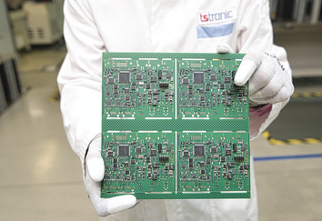
Automated optical inspection in PCB manufacturing: How AOI systems improve quality and efficiency
In the evolving landscape of electronics production, ensuring the accuracy, reliability, and efficiency of each component on a printed circuit board (PCB) is vital. Among the advanced technologies implemented across Surface Mount Technology (SMT) and Through-Hole Technology (THT) processes, Automated Optical Inspection (AOI) stands out as a critical pillar of quality assurance. AOI provides a non-contact, high-speed solution for defect detection, designed to meet the demands of increasingly complex PCB designs and shrinking component geometries.
The transition from manual inspection to automated inspection systems has significantly transformed how manufacturers approach quality control. Traditional visual inspection techniques, although still present in some manufacturing lines where manual inspection is applied, lack the speed and repeatability required by high-volume production. In contrast, AOI systems are commonly used in SMT lines to inspect thousands of solder joints and components in a matter of seconds, significantly speeding up the inspection process while reducing human error.
The role of AOI in electronics manufacturing is no longer supplementary it has become an essential inspection technology to ensure defect-free products and maximize throughput. From bare board inspection to post-reflow verification, AOI enables the detection of common defects such as misalignments, missing components, open circuits, and solder issues. As miniaturization trends continue, the need for precise, high-speed automated inspection grows in parallel.
This chapter presents a foundational understanding of AOI, its integration into PCB production, and its growing role in modern manufacturing. We will examine how AOI systems function, the evolution of AOI technology, and the specific challenges they are designed to address in modern PCB manufacturing environments.
Automated Optical Inspection (AOI) is an advanced inspection method used in electronics manufacturing to detect a wide variety of production defects by capturing and analyzing visual data from printed circuit boards (PCBs). AOI utilizes machine vision to compare a live image of a PCB or its components against a pre-defined standard or reference. Any deviation from this reference may indicate a fault, such as a missing component, incorrect placement, misalignment, or solder defect.
An AOI system used for PCB manufacturing typically includes a high-resolution optical system, advanced image processing algorithms, and often a combination of 2D and 3D AOI capabilities. The inspection takes place at various stages, including post-solder paste application, post-placement, and post-reflow, ensuring that each component is not only present but correctly aligned and properly soldered.
What distinguishes AOI systems from other forms of inspection equipment is their ability to deliver real-time, repeatable, and consistent results across high-volume production environments. AOI can inspect thousands of PCB assemblies per day, offering both speed and accuracy without the fatigue or inconsistency associated with manual visual inspection.
The evolution of AOI technology has been shaped by the growing demand for miniaturization, higher component densities, and reduced tolerance for manufacturing errors. Early AOI machines were limited in scope, focusing mainly on presence and absence checks. Over time, however, improvements in optical systems, lighting techniques, and processing software have transformed AOI into a powerful tool for complex fault detection.
Today’s automated optical inspection systems leverage advanced computational capabilities to perform inspections on both visible and hidden areas of a PCB board, identifying issues like lifted leads, insufficient solder joints, or polarity errors. Modern AOI systems also benefit from integration with production data systems, enabling real-time defect tracking and closed-loop feedback for process improvement.
This development has made AOI indispensable in high-density, high-speed manufacturing lines where manual inspection is no longer viable. The increased accuracy of both inspection equipment and image analysis has elevated AOI to a status where it not only detects but also helps to prevent faults by revealing trends and enabling proactive process adjustments.
In modern SMT lines, AOI plays a central role in ensuring product quality while supporting rapid throughput. As surface-mounted components become increasingly small and densely packed, the margin for error in PCB fabrication shrinks dramatically. AOI systems offer a solution by delivering high-speed automated inspections that are both precise and scalable.
One of the key reasons for AOI’s dominance in SMT environments is its ability to be placed at multiple points along the manufacturing line. It can be used after solder paste inspection, post-placement, or after reflow, serving as a safeguard at each critical juncture. For example, an AOI test after reflow soldering is essential to confirm that all components have formed reliable electrical connections and that no defects have developed due to thermal stress.
By ensuring that boards move to the next step of production without issues, AOI allows manufacturers to maintain tight control over the production line and your PCB quality. It helps reduce rework, improve first-pass yield, and limit costly downstream failures.
The manufacturing process of a printed circuit board (PCB) is a highly structured sequence of mechanical, chemical, and thermal operations that transform a bare substrate into a fully functional electronic platform. The journey begins with the selection of a suitable laminate, typically made from FR-4 or similar composite materials, which is then subjected to a range of treatments including copper plating, photoresist application, UV exposure, etching, drilling, and solder mask deposition.
As component miniaturization advances and interconnect density increases, PCB design has become more intricate, requiring highly precise fabrication techniques. Layer registration, drill accuracy, and trace fidelity must all meet stringent tolerances. Multilayer PCBs, in particular, demand careful alignment and via formation to ensure signal integrity.
Following fabrication, the board enters the PCB assembly stage, where components are mounted using either Surface Mount Technology (SMT) or Through-Hole Technology (THT). At each step, opportunities for errors—ranging from dimensional inaccuracies to material inconsistencies can arise. These risks underscore the necessity for robust inspection strategies, especially in high-volume environments where consistency and quality are paramount.
Automated Optical Inspection (AOI) is strategically integrated at multiple stages of PCB production to ensure that boards meet the required specifications before advancing through the manufacturing line. AOI systems are commonly deployed post-solder paste application, post-component placement, and post-reflow. Each placement provides a checkpoint where deviations from expected results can be identified and addressed before incurring additional costs.
At the solder paste inspection stage, AOI is used to verify that paste volumes are adequate and properly aligned. During component placement, AOI validates that each part is present, oriented correctly, and positioned within acceptable tolerances. Finally, after reflow soldering, AOI inspects for defects such as tombstoning, bridging, and cold solder joints.
The flexibility of AOI systems to adapt to various inspection stages provides manufacturers with a scalable solution for maintaining inspection efficiency. By implementing AOI early and often, manufacturers can detect issues in real time, allowing them to make adjustments that improve yields and reduce scrap. This level of control is especially critical in PCB fabrication areas where tight production cycles and minimal defect rates are essential.
Defects during the manufacturing process of PCBs can originate from several sources, including material flaws, machine calibration errors, process inconsistencies, or environmental conditions. Among the most prevalent issues are misaligned components, missing parts, solder bridging, insufficient solder, and open circuits. These defects compromise the electrical performance, mechanical integrity, and overall reliability of the final product.
In high-speed manufacturing lines where manual inspection is no longer feasible, these flaws can propagate rapidly, resulting in substantial production losses. Undetected errors at early stages often lead to complex failures later in the process or in the field, requiring costly repairs or replacements. For example, an undetected solder issue may only manifest during functional testing, complicating fault isolation and repair.
Moreover, certain defects may be intermittent or latent, escaping detection until after deployment. This creates risks in critical applications such as automotive, aerospace, or medical electronics, where failure can have severe consequences. Therefore, maintaining robust and accurate inspection methods, including AOI, is essential to ensuring the quality of the final product and safeguarding end-user trust.
The role of AOI in early-stage defect detection is crucial to maintaining quality control across the entire electronics production lifecycle. By inspecting boards at key transition points, AOI helps identify defects before they can accumulate and compromise downstream processes. The ability to halt defective products at the source allows manufacturers to protect their yield and reduce the cost associated with rework or scrapping.
One of the main advantages of AOI systems is their ability to perform board inspection at high speed with high accuracy. Leveraging sophisticated optical systems to identify defects, AOI provides a detailed, real-time snapshot of the product under inspection. This data, captured by the optical system, is processed and compared against reference models to detect even the most subtle deviations.
By detecting and classifying defects such as incorrect polarity, misplacement, or insufficient solder, AOI enables engineers to take corrective action during the same production cycle. In doing so, it enhances process control and supports the goal of producing PCBs without any manufacturing faults. AOI also enables traceability, contributing to better analytics and continuous improvement in production workflows.
Inspection in electronics manufacturing has traditionally relied on human visual verification. Manual inspection involves trained operators examining PCB assemblies to detect visible anomalies, such as missing components, misalignments, or poor solder joints. While this method offers flexibility and immediate feedback, it is inherently limited by fatigue, subjective judgment, and inconsistency. These limitations become more pronounced as component sizes shrink and board complexity increases.
In contrast, automated inspection systems such as AOI deliver objective, repeatable results with high throughput and resolution. These systems do not suffer from attention span or lighting variability, allowing them to identify defects more reliably in complex and densely populated boards. While manual visual inspection may still be used for prototype validation or final verification in low-volume contexts, it is increasingly being phased out of high-speed manufacturing lines where manual inspection is no longer viable.
The shift from manual to automated inspection methods marks a pivotal advancement in the industry’s drive for consistency, inspection efficiency, and traceability. It also underscores the growing importance of data-driven quality control, where processing software evaluates inspection results in real time, enabling corrective action within the same production cycle.
In the context of test and inspection methods for electronic assemblies, Automated Optical Inspection (AOI), X-ray inspection, and Solder Paste Inspection (SPI) serve complementary but distinct roles. AOI is primarily used for surface-level verification evaluating placement accuracy, component orientation, and solder quality visible to the optical system. Its strength lies in speed and precision, particularly for densely populated PCB boards where errors must be caught quickly.
X-ray inspection, on the other hand, is essential when verifying defects beneath components that AOI cannot reach, such as Ball Grid Arrays (BGAs) and other bottom-terminated packages. X-ray systems visualize internal connections and hidden solder joints, identifying issues like voids, insufficient solder, and internal bridging. Although slower and more expensive, X-ray provides invaluable insight in areas where AOI has physical limitations.
SPI systems are utilized before reflow soldering to inspect the volume, alignment, and height of applied solder paste. This is a preventive method to reduce solder-related defects later in the process.
While each system has its own specialty, a holistic inspection strategy often integrates multiple technologies. AOI provides fast, surface-level screening, while SPI and X-ray offer deeper diagnostics. The most effective inspection processes combine these technologies, ensuring both broad and deep coverage of potential failure points.
Among all inspection technologies available in the industry today, AOI stands out for its ability to deliver reliable and repeatable results across a variety of production environments. Using precise optical systems, advanced lighting schemes, and high-speed cameras, AOI systems typically identify defects that human eyes or simpler machines might miss. These include not only component presence and alignment, but also polarity issues, incorrect values, and subtle solder defects.
What makes AOI systems particularly effective is their adaptability. As PCB manufacturing processes evolve, AOI can be used with both legacy equipment and cutting-edge, fully automated lines. The use of historical defect data captured by AOI supports trend analysis and continuous improvement, making it a cornerstone of modern quality assurance frameworks.
Furthermore, the development of an AOI system now includes machine learning capabilities that allow inspection algorithms to adapt over time. This means that the system improves not just in speed, but also in defect classification accuracy, reducing false positives and enhancing process control.
By providing immediate feedback and data-rich reports, AOI supports process transparency, product reliability, and long-term cost efficiency. Its role is no longer limited to error detection it has become an active contributor to strategic decision-making in electronics production.
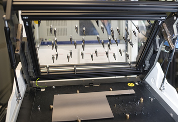
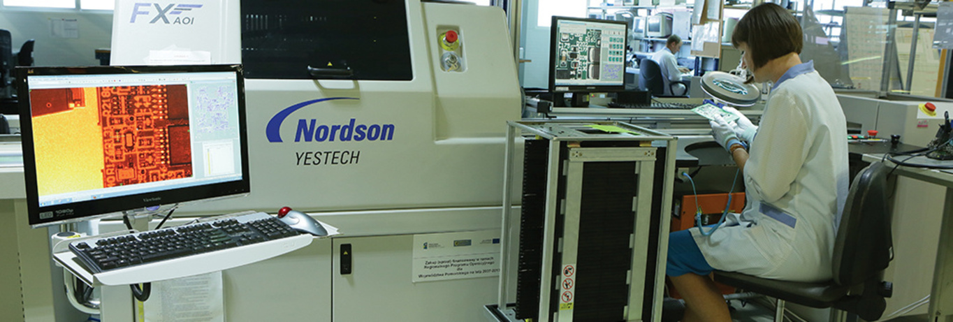
At the heart of every AOI system lies a fusion of advanced optics, image processing, and intelligent algorithms, enabling fast and accurate inspection of electronic assemblies. These systems utilize high-resolution cameras coupled with precision-controlled lighting setups to capture detailed images of the PCB or product under inspection. The images are then analyzed using powerful processing software, which compares them to a reference image or a digital model based on the original PCB design.
A key factor in the effectiveness of AOI is the quality of the optical system. Modern AOI machines employ multiple lighting angles, including coaxial and side lighting, to enhance contrast and highlight topographical features. The data captured by the optical system is used not only for simple presence or absence checks but also for geometric analysis of component shape, alignment, and solder coverage.
In high-density boards, positional precision is critical. An AOI system should have sub-pixel accuracy to detect slight variations that could lead to performance degradation or failures in the field. In advanced setups, 3D AOI technology provides height information, which is essential for evaluating component planarity and solder joint volume factors that cannot be reliably measured using 2D imaging alone.
By integrating real-time analytics with hardware control, automated optical inspection systems deliver consistent quality control even in the most demanding environments. This capability ensures manufacturers can keep pace with increasing manufacturing speeds, detect issues early, and maintain throughput without compromising product quality.
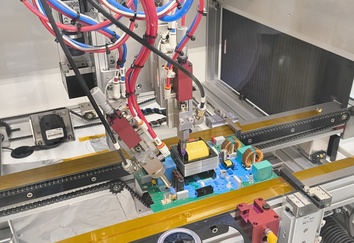
A typical AOI system used for PCB manufacturing is composed of several tightly integrated subsystems designed to work together seamlessly. These include an imaging unit, an illumination module, a mechanical stage, a computational core, and a user interface for programming and monitoring.
The imaging unit features industrial-grade cameras capable of capturing high-resolution images at fast frame rates. These cameras are paired with specialized lenses optimized for minimal distortion and maximum field of view. The illumination module, often comprising multiple LED arrays, is engineered to highlight surface features and enhance defect visibility by manipulating shadow and contrast.
The mechanical stage either fixed or movable ensures precise positioning of the PCB under the camera. Motion control systems with micron-level accuracy are essential for scanning large areas while maintaining inspection fidelity. The computational core houses the algorithms responsible for feature recognition, pattern matching, and defect classification. Depending on the system, artificial intelligence may be employed to improve classification accuracy and reduce false positives over time.
Finally, the human-machine interface (HMI) allows operators to define inspection criteria, load reference models, review flagged defects, and generate reports. It also facilitates integration with inspection equipment and manufacturing databases, enabling traceability and closed-loop feedback within the EMS production environment.
The demand for high-speed automated inspection solutions has led to the development of AOI platforms that operate in real-time on SMT lines. These systems are optimized for rapid throughput, ensuring that every PCB on the line undergoes comprehensive inspection without slowing down production. High-speed AOI systems combine short image acquisition times with fast processing algorithms and hardware acceleration to meet the requirements of high-speed manufacturing lines where manual inspection is no longer feasible.
To ensure thorough inspection in these dynamic environments, modern AOI systems must balance speed with accuracy. This includes using stroboscopic lighting to eliminate motion blur, high-frame-rate cameras to capture more data per second, and intelligent algorithms that prioritize critical inspection points based on historical failure data.
The capability of AOI systems to inspect components at high speeds without compromising quality is crucial for efficiency in modern manufacturing. These systems reduce bottlenecks and increase first-pass yield, contributing to leaner operations and improved resource utilization. Furthermore, their inspection capabilities and volumetric inspection data allow engineers to monitor process stability over time and respond proactively to deviations.
In EMS environments, where the complexity and volume of production are both high, the successful deployment of AOI systems depends on their seamless integration with existing processes and equipment. AOI must interface with upstream and downstream machinery to ensure synchronization of PCB movement, data capture, and quality control workflows.
An AOI system to keep pace with production requires robust mechanical design, reliable communication protocols, and compatibility with manufacturing execution systems (MES). This integration enables real-time defect logging, automated rework routing, and adaptive process tuning based on inspection feedback. In some cases, AOI and X-ray inspection are used in tandem to cover both visible and hidden elements of the assembly.
Moreover, the ability to deploy a single system that supports multiple inspection methods—such as pre-placement, post-placement, and post-reflow enhances production flexibility and minimizes floor space usage. By placing AOI at strategic checkpoints, manufacturers gain insight into process stability and can rectify the process when trends indicate systemic issues.
Ultimately, the integration of AOI enhances not only the quality of your PCB fabrication but also the traceability, accountability, and continuous improvement of the entire production ecosystem.
The implementation of Automated Optical Inspection (AOI) in SMT inspection has significantly enhanced the speed and accuracy of defect detection, resulting in increased overall inspection efficiency. Traditional manual inspection methods are time-consuming and prone to human error, particularly in high-density, small-form-factor assemblies. AOI, by contrast, performs real-time assessments using precision optical systems that capture and analyze detailed images of each PCB.
By leveraging predefined inspection criteria and algorithmic analysis, AOI systems eliminate variability, reduce inspection cycle times, and allow for continuous operation without operator fatigue. The ability to inspect each unit thoroughly and at high speed means that AOI can inspect thousands of boards per day while maintaining a consistent quality threshold.
As production volumes grow, the need for rapid and reliable inspection grows in parallel. AOI supports this scalability by offering modular configurations that adapt to line speed, board complexity, and throughput demands. This makes AOI a critical enabler of efficiency in modern manufacturing, particularly in environments where minimal downtime and maximum yield are essential.
One of the primary benefits of AOI is its ability to significantly reduce false positives and the inconsistencies introduced by human judgment. In manufacturing lines where manual inspection was once the standard, variability in lighting conditions, operator experience, and fatigue often led to missed or incorrectly flagged defects. These issues not only affect quality but also increase costs associated with unnecessary rework and investigation.
Modern AOI systems typically apply machine learning algorithms and statistical decision-making to distinguish true faults from process tolerances or cosmetic anomalies. This leads to more accurate inspection results and a lower incidence of false calls. Over time, AOI systems become more refined as they are trained on larger datasets, improving their capability to interpret complex features such as ambiguous solder joints or varying component textures.
By minimizing the human factor in visual inspection, AOI contributes to a more controlled and repeatable production process, which is especially important in applications where precision and reliability are non-negotiable.
Though the initial investment in an AOI system can be significant, its long-term value lies in the operational savings it enables. AOI provides a proactive quality control approach that prevents defects during the manufacturing process rather than correcting them post-production. This preventative strategy leads to reduced rework, fewer product returns, and less waste—all of which contribute to cost efficiency.
The speed and automation of AOI systems also translate to reduced labor costs, especially when replacing or supplementing manual visual inspection. Furthermore, detailed reporting capabilities support faster failure analysis and quicker root cause identification, leading to improved productivity across the entire PCB fabrication industry.
In addition, AOI enhances traceability. By logging defects and tracking their occurrence over time, manufacturers gain insight into process stability and equipment performance. This data-driven approach supports continuous improvement initiatives and can significantly reduce quality-related expenses over the product’s life cycle.
The primary goal of any inspection equipment is to ensure that only functional, high-quality assemblies proceed to the next stage of the production process. AOI fulfills this role by acting as a gatekeeper, preventing boards with critical defects such as component misplacement, polarity reversals, or poor solder connections from continuing down the line.
In environments with strict quality standards, AOI allows manufacturers to meet customer expectations consistently. Its ability to detect and classify a wide range of defects improves first-pass yield and reduces the number of boards requiring rework. Moreover, the statistical data generated by AOI can be used to optimize upstream processes, contributing to a closed-loop feedback system.
AOI also plays a vital role in the quality assurance strategies of high-reliability industries. Its contribution to maintaining the quality of your PCB fabrication cannot be overstated, particularly in applications where even a single failure can lead to system-wide consequences. By ensuring that every board is free from critical defects, AOI helps uphold product integrity from the factory floor to the end user.
Despite its many advantages, the deployment of Automated Optical Inspection (AOI) is not without challenges. One of the most common difficulties lies in the calibration and maintenance of the AOI system, which must be tailored to the specifics of the inspection task. Each type of PCB, assembly style, and component footprint demands a unique inspection configuration, including lighting angles, imaging resolution, and tolerance thresholds.
Another challenge relates to the positional accuracy of both inspection and placement systems. As components continue to shrink and layouts become more intricate, even minor deviations in alignment can trigger false calls or missed defects. Ensuring that the AOI machine maintains precise registration with the PCB is critical for consistent and accurate results.
Moreover, AOI systems can inspect a vast array of features, but their effectiveness can be reduced if the input design data is incomplete or inconsistent. Gerber files, component libraries, and assembly drawings must be harmonized to avoid discrepancies between the intended design and what the inspection machine expects to find. This makes the setup process time-intensive, particularly when working with highly customized or rapidly changing production runs.
Finally, environmental conditions such as vibration, lighting interference, or contamination on lenses can also degrade the performance of the optical inspection process. These factors underscore the need for ongoing equipment maintenance and process oversight in high-reliability manufacturing settings.
Selecting an appropriate AOI system involves more than evaluating camera resolution or scan speed. A comprehensive approach must consider the type of products being assembled, the layout of the production line, and the integration with existing equipment. In EMS facilities, this often includes compatibility with upstream placement machines and downstream reflow ovens, as well as the ability to interface with traceability systems and defect analytics software.
Different inspection needs require different configurations. For example, an AOI system requires different types of lighting and imaging setups depending on whether it is inspecting fine-pitch BGAs, connectors, or passive components. Systems must also account for variations in PCB surface finish, color, and reflectivity, which can impact image contrast and defect detectability.
Manufacturers must also determine whether they need a system to test and check solder paste deposition, component presence, or post-reflow conditions or all three. In some cases, investing in one comprehensive inspection system that supports multiple inspection phases can improve workflow efficiency and reduce equipment footprint.
Furthermore, considerations around scalability are crucial. As production ramps up, the AOI test can flexibly increase inspection capacity when designed with modularity in mind. This flexibility ensures that the inspection strategy evolves in tandem with changing production demands, without requiring complete system overhauls.
Although AOI systems are highly automated, effective use still depends on qualified personnel who understand both the technology and the production environment. Operators must be trained not only in how to use the interface and interpret inspection results, but also in how to optimize inspection parameters for varying products and defect types.
Proper training ensures that users can differentiate between true defects and cosmetic anomalies, reducing false calls and minimizing unnecessary rework. In addition, engineers should understand how to use AOI output data to rectify the process by identifying root causes and adjusting upstream parameters accordingly. This knowledge is key to maintaining quality and implementing feedback loops that improve yield over time.
Moreover, as inspection algorithms become more sophisticated, especially in systems that incorporate artificial intelligence, operators must develop skills in configuring and validating AI-based decision logic. In such systems, a deep understanding of vision inspection principles and pattern recognition helps avoid overfitting or underdetection.
Well-trained personnel are also critical for maintaining hardware and software performance. Preventive maintenance, calibration routines, and updates to component libraries are necessary for long-term AOI accuracy. In essence, while AOI reduces reliance on subjective human inspection, it simultaneously elevates the need for technical expertise in system management.
The continued advancement of Automated Optical Inspection (AOI) is shaped by demands for greater speed, accuracy, and adaptability in electronics manufacturing. One significant trend is the evolution toward automatic optical inspection systems that combine both 2D and 3D imaging. These hybrid solutions enable more detailed analyses of components and solder joints, ensuring accurate detection of volumetric and positional anomalies.
As miniaturization and component density increase, AOI systems must address the need for enhanced resolution, faster image capture, and intelligent data processing. In this context, one of the most critical innovations is the development of AOI systems that can inspect increasingly complex assemblies with minimal false positives. To meet this challenge, manufacturers are integrating adaptive lighting systems, high-frame-rate cameras, and more sophisticated algorithms capable of self-optimization over time.
Another emerging direction is modularity and scalability. An AOI system that requires different types of configuration based on board size, inspection depth, and process stage is becoming the new standard. Systems that are easily adaptable to new product introductions, layout changes, or reconfigured manufacturing lines, allow producers to maintain flexibility without sacrificing inspection reliability.
These trends reflect the industry's broader focus on manufacture and assembly with AOI as an integral, data-driven function not merely a checkpoint, but an evolving intelligence platform embedded within the production line.
Artificial intelligence and machine learning are fundamentally reshaping how AOI is implemented and optimized. Traditional AOI relies on rule-based comparisons between the PCB under review and a reference model. While effective, this method can struggle with components or board conditions that fall within acceptable but visually diverse ranges. Here, AI introduces the ability to learn from variations and interpret defects in a more contextual and probabilistic manner.
Modern systems are designed so that boards automatically undergo AOI, and the system continues to learn from the accumulated inspection data. This enables more accurate classification of previously ambiguous anomalies, enhancing the overall quality of inspection. The integration of machine learning allows AOI to respond dynamically to changing conditions on the line, effectively reducing false calls and increasing inspection speed without losing sensitivity.
By analyzing trends in real-time, AI-equipped AOI platforms can also assist in predictive maintenance, signaling when production drift might lead to defects. These insights are valuable not only for immediate corrections but also for long-term process improvements.
Such developments support the future of AOI as a vision inspection technology that goes beyond static rule application, evolving instead into a diagnostic tool that interacts with the full scope of PCB fabrication variables.
In the era of Industry 4.0, AOI plays a pivotal role in enabling real-time, interconnected manufacturing ecosystems. Smart factories demand autonomous systems that do more than inspect; they must communicate, adapt, and contribute to systemic efficiency. This places AOI at the core of system to test and check quality, guide robotic correction, and provide traceable data across the production chain.
A fully integrated AOI platform contributes to process orchestration by capturing quality metrics in real time and feeding that data into the manufacturing execution system (MES). This allows for closed-loop feedback that helps to maintain the quality and rectify the process immediately when trends or outliers are detected.
Additionally, assembly with AOI and X-ray technologies is becoming more common in high-reliability sectors where surface and subsurface defects must be simultaneously assessed. In these configurations, AOI ensures surface precision, while X-ray systems validate internal structural integrity together forming a robust, multi-layered inspection environment.
As smart factories continue to evolve, AOI's role expands from a standalone tool into a node within a larger, autonomous ecosystem. The result is a manufacturing environment where each inspection machine becomes both a quality gate and a data source, enabling predictive analytics and process self-correction.
Throughout the entire lifecycle of PCB production, from bare board fabrication to final assembly, Automated Optical Inspection (AOI) serves as a critical checkpoint and diagnostic mechanism. Its role has expanded from simple visual verification to an integrated, intelligent system capable of analyzing, learning, and reacting to changing manufacturing conditions. In modern EMS environments, AOI is not only an inspection tool but also an enabler of real-time process control and strategic quality management.
As the complexity of electronics grows and tolerances narrow, the importance of reliable, repeatable, and high-speed inspection becomes undeniable. AOI has proven itself as an important inspection system to test the structural and functional integrity of assemblies, minimizing the risk of latent failures and reinforcing confidence in downstream performance. With its capacity to identify and classify a wide range of defects, AOI ensures that only boards conforming to design intent and quality standards continue through the production line.
Moreover, as automation continues to redefine electronics manufacturing, AOI’s role becomes increasingly central to ensuring PCBs without any manufacturing faults reach the end user. It stands as one of the most powerful tools for achieving precision and consistency in environments where traditional inspection techniques fall short.
For manufacturers seeking to optimize quality and throughput in PCB assembly, the integration of AOI systems is no longer optional it is essential. AOI bridges the gap between manual skill and digital precision, ensuring that every board meets stringent performance criteria while contributing to a broader culture of process accountability.
When used in PCB fabrication, AOI allows for early intervention and detailed traceability, enabling teams to take corrective actions before defects propagate. The technology supports scalable production strategies and is particularly well-suited to high-speed, automated environments, where demand for reliability must be met without compromising efficiency.
It is worth noting that optical inspection is a visual technology at its core. However, its evolution into a data-rich, intelligent process control tool has elevated it far beyond its original scope. In today’s landscape, solutions like automated optical inspection provide not only visibility into production but also actionable insights that drive continuous improvement.
In conclusion, AOI stands at the intersection of quality assurance, manufacturing efficiency, and technological innovation. Its ability to detect, analyze, and adapt ensures that modern electronic products are built with precision, verified with confidence, and delivered with integrity.